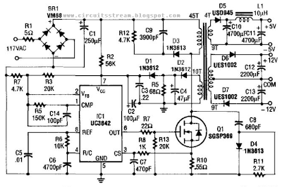
Circuit diagram:
Thursday, January 9, 2014
100Khz Multiple Output Switching Power Supply Circuit Diagram

Friday, December 27, 2013
Build a 5v And 12V Ac Powered Switching Supply Circuit Diagram

Thursday, December 26, 2013
Simple Micro volt probe Circuit Diagram

Tuesday, December 24, 2013
Build a High voltage Bucking Regulator Circuit Diagram

Saturday, December 21, 2013
Build a High Voltage Dc Generator Circuit Diagram

Sunday, October 6, 2013
Amplifier Timer Circuit Diagram
R1,R8___________1K 1/4W Resistors
R2,R3___________4K7 1/4W Resistors
R4_____________22K 1/4W Resistor
R5______________4M7 1/4W Resistor
R6,R9__________10K 1/4W Resistors
R7______________1M5 1/4W Resistor
R10___________100K 1/4W Resistor
R11____________15K 1/4W Resistor
R12____________10M 1/4W Resistor
R13_____________1M 1/4W Resistor
R14_____________8K2 1/4W Resistor
R15_____________1K8 1/4W Resistor
C1____________470µF 25V Electrolytic Capacitor
C2,C3,C6______100nF 63V Polyester Capacitors
C4,C5__________10µF 25V Electrolytic Capacitors
D1_____Diode bridge 100V 1A
D2,D7________1N4002 100V 1A Diodes
D3__________Red LED 5mm.
D4_______Yellow LED 5mm.
D5,D6________1N4148 75V 150mA Diodes
IC1___________78L12 12V 100mA Voltage regulator IC
IC2___________LM358 Low Power Dual Op-amp
IC3____________4060 14 stage ripple counter and oscillator IC
Q1____________BC557 45V 100mA PNP Transistor
Q2____________BC337 45V 800mA NPN Transistor
J1______________RCA audio input socket
P1_____________SPST Mains suited Pushbutton
P2_____________SPST Pushbutton
T1_____________220V Primary, 12V Secondary 3VA Mains transformer
RL1___________10.5V 270 Ohm Relay with SPST 5A 220V switch
PL1____________Male Mains plug
SK1__________Female Mains socket
Notes:
- Simply connect left or right channel tape output of your amplifier to J1.
- You can employ two RCA input sockets wired in parallel to allow pick-up audio signals from both stereo channels.
- The delay time can be varied changing R13 and/or C6 values.
- Needing to operate a device not supplied by power mains, use a double pole relay switch, connecting the second pole switch in series to the device supply.
Saturday, October 5, 2013
Logic Probe With Sound Circuit
This logic probe can be selected to operate on TTL or CMOS logic levels, depending on switch S1. A string of resistors associated with switch S1 sets the threshold levels for a window comparator comprising IC1a and IC1b. Depending on whether the level applied to the probe is high or low, the window comparator turns on LED1 (high) or LED2 (low). The 1.2M and 680k resistors set the probe signal to a midrange value when the probe is open-circuit, thereby preventing either LED from being lit.
Circuit diagram:
Logic Probe With Sound Circuit digram
If a pulse signal is present, the output of IC1a will toggle the clock input of flipflop IC2a. This drives LED3 which either lights for each pulse or continuously, depending on the setting of switch S2. Finally, the outputs of IC1a & IC1b are connected by diodes D5 & D6 to the base of transistor Q1 which is connected to the Reset input of flipflop IC2b. This has a piezo sounder (not buzzer) connected between its Q and Q-bar outputs so that it produces a sound which echoes the input pulse signal.
Author: Tom Hughes Copyright: Silicon Chip Electronics
Friday, October 4, 2013
Aviation Intercom Circuit
Before its move offshore, I was lucky enough to be involved in developing the avionics system for the Flightship Ground Effect FS8 craft (see www.pacificseaflight.com/craft.shtml). Although officially classed as a boat, it has wings and can travel at 180km/h some three metres above the water. The communications system was adapted from an aircraft unit and was a particular problem. It was expected to allow speech between the two pilots and radio, as well as receive audible warnings from the onboard computers and feed sound to the onboard data logger. Initially, the system was very noisy due to ground loops and incompatibility problems.
A circuit similar to that shown here was the solution. Although optimised to suit Softcom brand headphones with active noise reduction, it should be suitable for most aviation sets. The plugs indicated are standard aviation types but are insulated from the instrument panel to eliminate earth loops. The inputs from the two pilots microphones are summed and amplified by transistors Q1 & Q2. When one pilot presses his or her transmit key (mounted on the yoke), the transmit relay (RLY1) closes, muting the other pilot’s microphone via the optocoupler (OPTO1).
Circuit diagram:
Aviation Intercom Circuit Diagram
The outputs from the microphone preamp, computer audio transformer (T1) and radio speaker transformer (T2) are summed via 10kΩ resistors and applied to the input of IC1, an LM386 audio amplifier. Note that transformers are used here to avoid creating additional earth loops. The output of the LM386 drives the pilots’ headphones via transformers T3 & T4, which are needed for impedance matching. Each audio source has its own level control (VR1, VR3 & VR4). The main volume control (VR5) is included to allow for ambient noise level. VR2 is used to set the signal level for the data logger.
Author: Gary Smith Copyright: Silicon Chip Electronics
Monday, September 30, 2013
Bass Booster Circuit
Increase the bass output of your present instrument at modest cost!
Bass Boost is todays sound... whether its the driving, gut-vibration pulsation of disco, or the solid bass line of soft, hard, or laid-back rock. One way to get the modern bass-boost sound without running out and buying an all-new expensive piece of equipment is to use a Bass Booster between your guitar, electronic organ or what-have-you, and the instrument amplifier. A bass booster strips the highs from the instruments output signal and amplifies low frequencies, feeding on "all-bass" sound to the instrument amplifier. Naturally, the bigger the speaker used with the amp, the more powerful the bass: use 15-inchers with the Bass Booster and you can rattle the windows. Bass Booster is powered by an ordinary 9 volt transistor radio battery. It can be assembled on a small printed board or on a veroboard using point to point wiring. The booster connects between your instrument and its amplifier through two standard RCA Jacks.
Circuit Diagram:
Parts:
P1 = 50K
P2 = 100K
R1 = 22K
R2 = 470K
R3 = 47K
R4 = 10K
R5 = 470R
R6 = 1K
Q1 = 2N2222
C1 = 2.2uF-25v
C2 = 100nF-63v
C31 = 00nF-63V
C4 = 3.3uF-25v
C5 = 470uF-25v
D1 = 5mm. Red Led
Q1 = 2N2222
B1 = 9v Battery
J1 = RCA Audio Input Socket
J2 = RCA Audio Output Socket
S1 = On-Off Switch
Using Bass Booster:
Connect your electronic guitar or other electronic instrument to input jack J1; Connect output jack J2 to your instruments amplifiers normally-used input. With power switch S1 off, key S2 so the instrument feeds directly to the instrument amplifier. With P2 set full counter-clockwise (Off), turn power switch S1 on, key S2 once, and advance P2 for the desired Bass Boost level. To cut back to natural sound just stomp down on S2 and key the Bass Booster out. Dont worry about leaving power switch S1 on for several hours of a gig. The circuit pulls less than 1mA from the battery, so battery will last many, many months.
source :www.extremecircuits.net
Wednesday, September 4, 2013
Electronic Security Door Key Circuit
Description
- R1-7-9=1Kohm
- R2-3-4-5=100Kohm
- R6 =10Kohm
- R9 =47Kohm
- IC1 = 4066
- IC2 =4N25
- Q1-2=BC550
- S1...11=Push button sw or keyboard
- S12=Push button normal closed
- All resistors is 1/4W 5%
Source Sam Electronic Circuits
Sunday, September 1, 2013
24 Second Shot Clock Circuit
This is a circuit intended to be used in basketball shot clock
Circuit Diagram
To start in 24 seconds; 24s LOAD SW and Reset SW should be push simultaneously. If not, the count will start in 99. Pulse input can be connected to 555 astable multivibrator but must be calibrated for real time clock. The PAUSE SW must have a Switch Debouncer so that the counter will count normal when counting is paused and then turn-on.
When the count reach 00, the NOR gate will have an output of logic1 that will turn on the two transistor. The buzzer will rung and light will turn on. The two transistors are continuously turn-on not until LOAD SW and Reset SW is push. All have a +5v power supply.
Wednesday, August 14, 2013
Build a Low pass filter Circuit Diagram
Low-pass filter Circuit Diagram

Sunday, August 11, 2013
Input Impedance Booster Circuit
Circuit diagram:
Thursday, August 8, 2013
USB Battery Charger Circuit Rise
Low-Power Bus The low power bus powered functions derived all its power from the VBUS and must not draw over one unit load (100mA) according to the USB standard. It must even be able to work between the VBUS voltage of four.40V and five.25V.
Self-Power Self power functions can draw up to 100mA from the VBUS and the rest from its outside source. This is the most simplest to design.
Wednesday, August 7, 2013
Protectors Circuit on SMPS power supply
| SMPS Circuit |
- Over voltage protector (OVP)
- Over current protector (OCP)
- Over load protector
- Short circuit protector
- Over temperature protector
Tuesday, August 6, 2013
170W AMPLIFIER BTL LM4651 LM4652 CIRCUIT DIAGRAM

- Supply Voltage ± 22V
- Output Current (LM4652) 10A
- Power Dissipation (LM4651) 1.5W
- Power Dissipation (LM4652) 32W
- ESD Susceptibility (LM4651) 2000V,
- ESD Susceptibility LM4652 (pins 2,6,10,11) 500V
- ESD Susceptibility (LM4651) (Note 5) 200V
- ESD Susceptibility LM4652 (pins 2,6,10,11) 100V
- Junction Temperature 150°C
- Soldering Information N, TA and TF Package (10 seconds) 260°C
- Storage Temperature -40°C to + 150°C
Saturday, August 3, 2013
Door Handle Alarm Circuit Using Transistor

The transistor Q1 is wired as an astable multi vibrator whose output is used to bias transistor Q2 to conduction. As a result the transistor q3 and LED are in OFF state. When someone touches the handle, the capacitance of the human body damps the oscillations of Q1.The cuts the biasing of Q2 and it goes OFF.As a result the current flows to the base of Q3 , it conducts and LED glows. If the switch S1 is ON the transistor pairs Q4&Q4 which is wired in the latching mode is triggered and the Buzzer Z1 is activated. When the person removes his hand from door handle the LED goes OFF but the buzzer continues to beep. The only way to mute the buzzer is to open the switch S2. All capacitors must be rated 15V.
A 9V battery or 9V DC power supply can be used to power the circuit. To make L1 wind 25 turns of 0.4 mm enameled copper wire on resistor R2 and solder the ends of the wire to the resistor leads. This unit will stand for the R2 as well as L1 because both are parallel in the circuit. A readily available 10mH inductor can be used for L2. Connect the point A in the circuit to the door handle using a long wire.
Thursday, August 1, 2013
Super Ni Cd Battery Charger 12 18V Circuit Diagram

Datasheet file1: Click here to download LM741.pdf datasheet.
Wednesday, June 12, 2013
Playback Amplifier For Cassette Deck circuit schematic with explanation
Circuit diagram:
Because of the symmetrical ±12 V supply lines, the capacitor will not be charged. If a single supply is used, the initial surge when the capacitor is being charged causes a loud click in the loudspeaker and, worse, magnetizes the tape. The playback head provides an audio signal at a level of 200–500 mV. The two amplifiers raise this to line level, not linearly, but in accordance with the RIAA equalization characteristic for tape recorders. Broadly speaking, this characteristic divides the frequency range into three bands:
- Up to 50 Hz, corresponding to a time constant of 3.18 ms, the signal is highly and linearly amplified.
- Between 50 Hz and 1.326 kHz, corresponding to a time constant of 120 µs, for normal tape, or 2.274 kHz, corresponding to a time constant of 70 µs, for chromium dioxide tape, the signal is amplified at a steadily decreasing rate.
- Above 1.326 kHz or 2.274 kHz, as the case may be, the signal is slightly and linearly amplified. This characteristic is determined entirely by A1 (A1’). To make the amplifier suitable for use with chromium dioxide tape, add a double-pole switch (for stereo) to connect a 2.2 kΩ resistor in parallel with R3 (R3’). The output of A1 (A1’) is applied to a passive high-pass rumble filter, C3-R5 (C3’-R5’) with a very low cut-off frequency of 7 Hz. The components of this filter have exactly the same value as the input filter, C1-R1 (C1’-R1’). The second stage, A2 (A2’) amplifies the signal ´100, that is, to line level (1V r.m.s.).
LM4906 Boomer Audio Power Amplifier circuit and epxlanation
In addition, no output coupling capacitors or bootstrap capacitors are required which makes the LM4906 ideally suited for cellphone and other low voltage portable applications. The LM4906 features a low-power consumption shutdown mode (the part is enabled by pulling the SD pin high). Additionally, an internal thermal shutdown protection mechanism is provided. The LM4906 also has an internal selectable gain of either 6 dB or 12 dB. A bridge amplifier design has a few distinct advantages over the single-ended configuration, as it provides differential drive to the load, thus doubling output swing for a specified supply voltage. Four times the output power is possible as compared to a single-ended amplifier under the same conditions (particularly when considering the low supply voltage of 5 to 6 volts).
Circuit diagram:
When pushed for output power, the small SMD case has to be assisted in keeping a cool head. By adding copper foil, the thermal resistance of the application can be reduced from the free air value, resulting in higher PDMAX values without thermal shutdown protection circuitry being activated. Additional copper foil can be added to any of the leads connected to the LM4906. It is especially effective when connected to VDD, GND, and the output pins. A bridge configuration, such as the one used in LM4906, also creates a second advantage over single-ended amplifiers. Since the differential outputs, Vo1 and Vo2, are biased at half-supply, no net DC voltage exists across the load.
This eliminates the need for an output coupling capacitor which is required in a single supply, single-ended amplifier configuration. Large input capacitors are both expensive and space hungry for portable designs. Clearly, a certain sized capacitor is needed to couple in low frequencies without severe attenuation. But in many cases the speakers used in portable systems, whether internal or external, have little ability to reproduce signals below 100 Hz to 150 Hz. Thus, using a large input capacitor may not increase actual system performance. Also, by minimizing the capacitor size based on necessary low frequency response, turn-on pops can be minimized.

