Showing posts with label power. Show all posts
Showing posts with label power. Show all posts
Thursday, January 9, 2014
100Khz Multiple Output Switching Power Supply Circuit Diagram
The 100Khz Multiple Output Switching Power Supply Circuit Diagram uses two VN4000A 400-V MOSPOWER FETs in a half-bridge power switch configuration. Outputs available are + 5 Vat 20 A and ±15 V (or ±12 V) at 1 A. Since linear three-terminal regulators are used for the low-current outputs, either ±12 V or ±15 V can be made available with a simple change in the transformer secondary windings.
A TU94 switching regulator IC proVides pulse-width modulation control and drive signals for the power supply. The upper MOSPOWER FET, Q7. in the power switch stage is driven by a simple transformer drive circuit. The lower MOS. Q6, since it is ground referenced. is directly driven from the control !C.
100Khz Multiple Output Switching Power Supply Circuit Diagram

Friday, September 27, 2013
Fully Adjustable Power Supply
Based on a National Semiconductor application note, this circuit uses an LM317 3-terminal regulator (REG1), chosen because of its built-in over-current and over-temperature protection. Its output is boosted up to just over 5A by the MJ2955 transistor (Q1). The output voltage is varied by adjusting the voltage on REG1’s ADJ terminal using VR1 (a 10kO potentiometer), via the 270O resistor. Adjustable current limiting is provided by op amp IC1, used as a comparator, which monitors the voltage across the 0.1O current sensing resistors. Once this voltage exceeds a level set by potentiometer VR2, then its output goes low, dragging down the adjust pin of REG1 and thus the output voltage.

LED1 illuminates when current limiting is occurring. The 10kO voltage adjust potentiometer (VR1) has one side connected to -5V instead of 0V so that the output voltage can be varied down to 0V instead of 1.2V (normal limit of an LM317). Trimpot VR3 is adjusted to set the minimum output voltage to +100mV or so. Note that because the -5V rail is used as a reference, it should be regulated using an LM7905 or similar. The LM317 3-terminal regulator and Q1 should be mounted on the same heatsink to take advantage of REG1’s thermal control.
Continue reading...

LED1 illuminates when current limiting is occurring. The 10kO voltage adjust potentiometer (VR1) has one side connected to -5V instead of 0V so that the output voltage can be varied down to 0V instead of 1.2V (normal limit of an LM317). Trimpot VR3 is adjusted to set the minimum output voltage to +100mV or so. Note that because the -5V rail is used as a reference, it should be regulated using an LM7905 or similar. The LM317 3-terminal regulator and Q1 should be mounted on the same heatsink to take advantage of REG1’s thermal control.
Friday, September 20, 2013
Fuse Box BMW 733i 1982 Diagram And Power Distribution Fuse Box Map
Fuse Box BMW 733i 1982 Diagram And Power Distribution Fuse Box Map - Here are new post for Fuse Box BMW 733i 1982 Diagram And Power Distribution Fuse Box Map.


Glove Box Light; Heated Door Lock; Ignition Key Warning/Seatbelt Warning; Interior Lights; Lights:Turn/Hazard Warning; On-Boar Computer; Radio/Power Antenna; Active Check Control; Dash Lights; Front Park/Tail/Underhood Light; Rear Marker/LicenseLights; Active Check Control; Backup Lights/Transmission Range Lights; Brake Lining Warning; Cruise Control; Dash Lights; Gauges; Idle Speed Control; Interior Lights; Power Mirrors; Power Windows; Trunk Light, Fuel Delivery/Evaporative Control; Idle Speed Control, Headlights , Cigar Lighters, Active Check Control; Auto Charging Flashlight; Central Locking; Gauges; Radio/Power Antenna; Stoplights/Cruise Control; Warning Indicators, Rear Defogger/Sunroof, Automatic Heater-Air Conditioner; Auxiliary Fan; Vacuum pump, FOglights(RH), Seatbelt Warning; Speedometer; Warning Indicators, Headlights,
Continue reading...
Fuse Box BMW 733i 1982 Diagram And Power Distribution Fuse Box Map


Glove Box Light; Heated Door Lock; Ignition Key Warning/Seatbelt Warning; Interior Lights; Lights:Turn/Hazard Warning; On-Boar Computer; Radio/Power Antenna; Active Check Control; Dash Lights; Front Park/Tail/Underhood Light; Rear Marker/LicenseLights; Active Check Control; Backup Lights/Transmission Range Lights; Brake Lining Warning; Cruise Control; Dash Lights; Gauges; Idle Speed Control; Interior Lights; Power Mirrors; Power Windows; Trunk Light, Fuel Delivery/Evaporative Control; Idle Speed Control, Headlights , Cigar Lighters, Active Check Control; Auto Charging Flashlight; Central Locking; Gauges; Radio/Power Antenna; Stoplights/Cruise Control; Warning Indicators, Rear Defogger/Sunroof, Automatic Heater-Air Conditioner; Auxiliary Fan; Vacuum pump, FOglights(RH), Seatbelt Warning; Speedometer; Warning Indicators, Headlights,
Tuesday, September 10, 2013
12V to 20V Automotive Power Converter
12V to +-20V Automotive Power Converter Diagram

The limitation of car supply voltage (12V) forces to convert the voltages to higher in order to power audio amplifiers. In fact the max audio power x speaker (with 4 ohm impedance) using 12V is (Vsupply+ - Vsupply-)^2/(8*impedance) 12^2/32 = 4.5Watts per channel, that is laughable... For powering correctly an amplifier the best is to use a symmetric supply with a high voltage differential. for example +20 - -20 = 40Volts in fact 40^2/32 = 50 Watts per channel that is respectable. This supply is intended for two channels with 50W max each (of course it depends on the amplifier used). Though it can be easily scaled up or the voltages changed to obtain different values.
Saturday, August 10, 2013
All Constructing Various DC Power Supplies Projects

One of the basic building blocks of electronics project is building your own DC power supplies from an AC source of 110 V.A.C or 220 V.A.C.The common DC voltages that are necessary to power up the devices are usually in the range of three V DC to 30 V DC. Usually the fixed types of DC voltages are 5V, 9V, 12V, 15V & 18V DC. With the advancement of know-how, lots of devices are using one.8 V DC these days. S M P S is becoming common these days as the demand for miniaturization due to space constraints increases.
Take note that for linear power supply projects, you need to make use of a step down power transformer to step down the AC voltage from the line voltage of 110 V.A.C or 220 V.A.C before using it to supply to the diode bridge.
Wednesday, August 7, 2013
Protectors Circuit on SMPS power supply
The simplest example SMPS which still uses 3 transistors (C3807, A1015 and power transistors) classic problem that often occurs is: - Problem in the feedback circuit can cause the output voltage B + over so that it can endanger the aircraft as a whole. For example elco erupted, pcb burnt burnt by over-heated, horizontal transistor short.
- Problem on feedback circuits may cause power regulator transistor is damaged due to over current transistor (eg, due to the 47k resistor transistor circuit on the secondary error detector value is delayed).
- If the input ac voltage drops can cause the power regulator transistor is damaged, due to over current transistor If the secondary there is a power transistor short can cause damage over current regulator.
- Protectors are designed to make the SMPS SMPS "reliable will not be damaged" if there are things that go wrong as mentioned above.
 |
| SMPS Circuit |
SMPS circuit using IC systems generally are designed with a surge protector, which include:
- Over voltage protector (OVP)
- Over current protector (OCP)
- Over load protector
- Short circuit protector
- Over temperature protector
Wednesday, June 12, 2013
LM4906 Boomer Audio Power Amplifier circuit and epxlanation
The well-known LM386 is an excellent choice for many designs requiring a small audio power amplifier (1-watt) in a single chip. However, the LM386 requires quite a few external parts including some electrolytic capacitors, which unfortunately add volume and cost to the circuit. National Semiconductor recently introduced its Boomer® audio integrated circuits which were designed specifically to provide high quality audio while requiring a minimum amount of external components (in surface mount packaging only). The LM4906 is capable of delivering 1 watt of continuous average power to an 8-ohm load with less than 1% distortion (THD+N) from a +5 V power supply. The chip happily works with an external PSRR (Power Supply Rejection Ratio) bypass capacitor of just 1 µF minimum.
In addition, no output coupling capacitors or bootstrap capacitors are required which makes the LM4906 ideally suited for cellphone and other low voltage portable applications. The LM4906 features a low-power consumption shutdown mode (the part is enabled by pulling the SD pin high). Additionally, an internal thermal shutdown protection mechanism is provided. The LM4906 also has an internal selectable gain of either 6 dB or 12 dB. A bridge amplifier design has a few distinct advantages over the single-ended configuration, as it provides differential drive to the load, thus doubling output swing for a specified supply voltage. Four times the output power is possible as compared to a single-ended amplifier under the same conditions (particularly when considering the low supply voltage of 5 to 6 volts).
Circuit diagram:

When pushed for output power, the small SMD case has to be assisted in keeping a cool head. By adding copper foil, the thermal resistance of the application can be reduced from the free air value, resulting in higher PDMAX values without thermal shutdown protection circuitry being activated. Additional copper foil can be added to any of the leads connected to the LM4906. It is especially effective when connected to VDD, GND, and the output pins. A bridge configuration, such as the one used in LM4906, also creates a second advantage over single-ended amplifiers. Since the differential outputs, Vo1 and Vo2, are biased at half-supply, no net DC voltage exists across the load.
This eliminates the need for an output coupling capacitor which is required in a single supply, single-ended amplifier configuration. Large input capacitors are both expensive and space hungry for portable designs. Clearly, a certain sized capacitor is needed to couple in low frequencies without severe attenuation. But in many cases the speakers used in portable systems, whether internal or external, have little ability to reproduce signals below 100 Hz to 150 Hz. Thus, using a large input capacitor may not increase actual system performance. Also, by minimizing the capacitor size based on necessary low frequency response, turn-on pops can be minimized.
In addition, no output coupling capacitors or bootstrap capacitors are required which makes the LM4906 ideally suited for cellphone and other low voltage portable applications. The LM4906 features a low-power consumption shutdown mode (the part is enabled by pulling the SD pin high). Additionally, an internal thermal shutdown protection mechanism is provided. The LM4906 also has an internal selectable gain of either 6 dB or 12 dB. A bridge amplifier design has a few distinct advantages over the single-ended configuration, as it provides differential drive to the load, thus doubling output swing for a specified supply voltage. Four times the output power is possible as compared to a single-ended amplifier under the same conditions (particularly when considering the low supply voltage of 5 to 6 volts).
Circuit diagram:

Boomer Audio Power Amplifier Circuit Diagram
When pushed for output power, the small SMD case has to be assisted in keeping a cool head. By adding copper foil, the thermal resistance of the application can be reduced from the free air value, resulting in higher PDMAX values without thermal shutdown protection circuitry being activated. Additional copper foil can be added to any of the leads connected to the LM4906. It is especially effective when connected to VDD, GND, and the output pins. A bridge configuration, such as the one used in LM4906, also creates a second advantage over single-ended amplifiers. Since the differential outputs, Vo1 and Vo2, are biased at half-supply, no net DC voltage exists across the load.
This eliminates the need for an output coupling capacitor which is required in a single supply, single-ended amplifier configuration. Large input capacitors are both expensive and space hungry for portable designs. Clearly, a certain sized capacitor is needed to couple in low frequencies without severe attenuation. But in many cases the speakers used in portable systems, whether internal or external, have little ability to reproduce signals below 100 Hz to 150 Hz. Thus, using a large input capacitor may not increase actual system performance. Also, by minimizing the capacitor size based on necessary low frequency response, turn-on pops can be minimized.
Friday, April 12, 2013
4 X 15 Watt Mini Power Amplifier
A lot of electronic circuits in the domain of audio amplifiers are already been published here. This circuit is a little different because it is a four channel amplifier. Each channel of this amplifier can deliver an output of 15Watts into a 4 ohm speaker. The amplifier can be operated from a single 12V DC supply and this makes it possible to use this amplifier in car audio applications too.
Circuit diagram :

4 X 15 Watt Mini Power Amplifier
The circuit is based on the 15W BTL X 2 channel audio power amplifier IC TA8215 from Toshiba. Even though chip is specifically designed for car audio applications it can be also used for home audio applications. Two TA8215 ICs are used here in order to obtain a 4 channel amplifier system. The circuit is designed almost exactly as per the application diagram in the ICs datasheet. Pins 7 and 19 are the Vcc pins of the ICs internal integrated power amplifier stages and these pins are connected to the positive supply. Pin 9 is the Vcc pin for ICs internal preamplifier and it is also connected to the positive supply. Pins 13 and 14 are the internal power amplifiers ground pins and they are tied together and connected to the ground.
The internal preamplifier’s ground pin (pin5) is connected to the common ground through a 10 Ohm resistor which makes the input ground separated from the common ground by a resistance of 10 ohms and this improves the noise rejection. The 100uF capacitor works as a power supply de-coupler. The resistor networks connected to the output lines of each amplifier improves the high frequency stability. The variable resistors (R3, R4, R12 and R13) works as the volume controller for the corresponding channels.
Notes :
- Assembling the circuit on a good quality PCB is a must for obtaining optimum sound quality.
- Use 12V DC for powering the circuit.
- The ICs must be fitted with adequately sized heat sinks.
- R3, R4, R12 and R13 serves as volume controllers.
- K1 to K4 can be 4 Ohm, 20W speakers.
- This amplifier circuit can be used in a variety of applications such as car audio systems, home theater systems, personal audio systems, public address systems etc. link
Wednesday, April 10, 2013
5 Volt Switching Regulator Power Supply
The switching regulator power supply used LM2575-5.0 on this schematic. You can make the stable voltage by using the 3 terminal regulator like LM317. However, because the output electric current and the inputted electric current are the same approximately, the difference between the input electric power (The input voltage x The input electric current) and the output power (The output voltage x The output current) is consumed as the heat with the regulator. Because it is, the efficiency isn�t good.
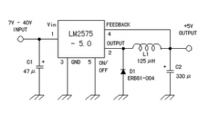
Data sheet for LM2575
SIMPLE SWITCHER 1A Step-Down Voltage Regulator
http://www.national.com/pf/LM/LM2575.htm
Monday, April 8, 2013
30 VDC Stabilized power supply with current control 0 002 3 A
General Description
This is a high quality power supply with a continuously variable stabilised output adjustable at any value between 0 and 30VDC. The circuit also incorporates an electronic output current limiter that effectively controls the output current from a few milliamperes (2 mA) to the maximum output of three amperes that the circuit can deliver. This feature makes this power supply indispensable in the experimenters laboratory as it is possible to limit the current to the typical maximum that a circuit under test may require, and power it up then, without any fear that it may be damaged if something goes wrong.
There is also a visual indication that the current limiter is in operation so that you can see at a glance that your circuit is exceeding or not its preset limits.Link
Technical Specifications - Characteristics
Input Voltage: ................ 24 VACHow it Works
Input Current: ................ 3 A (max)
Output Voltage: ............. 0-30 V adjustable
Output Current: ............. 2 mA-3 A adjustable
Output Voltage Ripple: . 0.01 % maximum
FEATURES
- Reduced dimensions, easy construction, simple operation.
- Output voltage easily adjustable.
- Output current limiting with visual indication.
- Complete protection of the supplied device against over loads and malfunction.

To start with, there is a step-down mains transformer with a secondary winding rated at 24 V/3 A, which is connected across the input points of the circuit at pins 1 & 2. (the quality of the supplies output will be directly proportional to the quality of the transformer). The AC voltage of the transformers secondary winding is rectified by the bridge formed by the four diodes D1-D4. The DC voltage taken across the output of the bridge is smoothed by the filter formed by the reservoir capacitor C1 and the resistor R1. The circuit incorporates some unique features which make it quite different from other power supplies of its class. Instead of using a variable feedback arrangement to control the output voltage, our circuit uses a constant gain amplifier to provide the reference voltage necessary for its stable operation. The reference voltage is generated at the output of U1. The circuit operates as follows: The diode D8 is a 5.6 V zener, which here operates at its zero temperature coefficient current. The voltage in the output of U1 gradually increases till the diode D8 is turned on. When this happens the circuit stabilises and the Zener reference voltage (5.6 V) appears across the resistor R5. The current which flows through the non inverting input of the op-amp is negligible, therefore the same current flows through R5 and R6, and as the two resistors have the same value the voltage across the two of them in series will be exactly twice the voltage across each one. Thus the voltage present at the output of the op-amp (pin 6 of U1) is 11.2 V, twice the zeners reference voltage. The integrated circuit U2 has a constant amplification factor of approximately 3 X, according to the formula A=(R11+R12)/R11, and raises the 11.2 V reference voltage to approximately 33 V. The trimmer RV1 and the resistor R10 are used for the adjustment of the output voltages limits so that it can be reduced to 0 V, despite any value tolerances of the other components in the circuit. Another very important feature of the circuit, is the possibility to preset the maximum output current which can be drawn from the p.s.u., effectively converting it from a constant voltage source to a constant current one. To make this possible the circuit detects the voltage drop across a resistor (R7) which is connected in series with the load. The IC responsible for this function of the circuit is U3. The inverting input of U3 is biased at 0 V via R21. At the same time the non inverting input of the same IC can be adjusted to any voltage by means of P2. Let us assume that for a given output of several volts, P2 is set so that the input of the IC is kept at 1 V. If the load is increased the output voltage will be kept constant by the voltage amplifier section of the circuit and the presence of R7 in series with the output will have a negligible effect because of its low value and because of its location outside the feedback loop of the voltage control circuit. While the load is kept constant and the output voltage is not changed the circuit is stable. If the load is increased so that the voltage drop across R7 is greater than 1 V, IC3 is forced into action and the circuit is shifted into the constant current mode. The output of U3 is coupled to the non inverting input of U2 by D9. U2 is responsible for the voltage control and as U3 is coupled to its input the latter can effectively override its function. What happens is that the voltage across R7 is monitored and is not allowed to increase above the preset value (1 V in our example) by reducing the output voltage of the circuit. This is in effect a means of maintaining the output current constant and is so accurate that it is possible to preset the current limit to as low as 2 mA. The capacitor C8 is there to increase the stability of the circuit. Q3 is used to drive the LED whenever the current limiter is activated in order to provide a visual indication of the limiters operation. In order to make it possible for U2 to control the output voltage down to 0 V, it is necessary to provide a negative supply rail and this is done by means of the circuit around C2 & C3. The same negative supply is also used for U3. As U1 is working under fixed conditions it can be run from the unregulated positive supply rail and the earth. The negative supply rail is produced by a simple voltage pump circuit which is stabilised by means of R3 and D7. In order to avoid uncontrolled situations at shut-down there is a protection circuit built around Q1. As soon as the negative supply rail collapses Q1 removes all drive to the output stage. This in effect brings the output voltage to zero as soon as the AC is removed protecting the circuit and the appliances connected to its output. During normal operation Q1 is kept off by means of R14 but when the negative supply rail collapses the transistor is turned on and brings the output of U2 low. The IC has internal protection and can not be damaged because of this effective short circuiting of its output. It is a great advantage in experimental work to be able to kill the output of a power supply without having to wait for the capacitors to discharge and there is also an added protection because the output of many stabilised power supplies tends to rise instantaneously at switch off with disastrous results.Construction
First of all let us consider a few basics in building electronic circuits on a printed circuit board. The board is made of a thin insulating material clad with a thin layer of conductive copper that is shaped in such a way as to form the necessary conductors between the various components of the circuit. The use of a properly designed printed circuit board is very desirable as it speeds construction up considerably and reduces the possibility of making errors. To protect the board during storage from oxidation and assure it gets to you in perfect condition the copper is tinned during manufacturing and covered with a special varnish that protects it from getting oxidised and also makes soldering easier.
Soldering the components to the board is the only way to build your circuit and from the way you do it depends greatly your success or failure. This work is not very difficult and if you stick to a few rules you should have no problems. The soldering iron that you use must be light and its power should not exceed the 25 Watts. The tip should be fine and must be kept clean at all times. For this purpose come very handy specially made sponges that are kept wet and from time to time you can wipe the hot tip on them to remove all the residues that tend to accumulate on it.
DO NOT file or sandpaper a dirty or worn out tip. If the tip cannot be cleaned, replace it. There are many different types of solder in the market and you should choose a good quality one that contains the necessary flux in its core, to assure a perfect joint every time.
DO NOT use soldering flux apart from that which is already included in your solder. Too much flux can cause many problems and is one of the main causes of circuit malfunction. If nevertheless you have to use extra flux, as it is the case when you have to tin copper wires, clean it very thoroughly after you finish your work.
In order to solder a component correctly you should do the following:
- Clean the component leads with a small piece of emery paper.
- Bend them at the correct distance from the components body and insert he component in its place on the board.
- You may find sometimes a component with heavier gauge leads than usual, that are too thick to enter in the holes of the p.c. board. In this case use a mini drill to enlarge the holes slightly. Do not make the holes too large as this is going to make soldering difficult afterwards.
- Take the hot iron and place its tip on the component lead while holding the end of the solder wire at the point where the lead emerges from the board. The iron tip must touch the lead slightly above the p.c. board.
- When the solder starts to melt and flow wait till it covers evenly the area around the hole and the flux boils and gets out from underneath the solder.
- The whole operation should not take more than 5 seconds. Remove the iron and allow the solder to cool naturally without blowing on it or moving the component. If everything was done properly the surface of the joint must have a bright metallic finish and its edges should be smoothly ended on the component lead and the board track. If the solder looks dull, cracked, or has the shape of a blob then you have made a dry joint and you should remove the solder (with a pump, or a solder wick) and redo it. Take care not to overheat the tracks as it is very easy to lift them from the board and break them.
- When you are soldering a sensitive component it is good practice to hold the lead from the component side of the board with a pair of long-nose pliers to divert any heat that could possibly damage the component.
- Make sure that you do not use more solder than it is necessary as you are running the risk of short-circuiting adjacent tracks on the board, especially if they are very close together.
- When you finish your work, cut off the excess of the component leads and clean the board thoroughly with a suitable solvent to remove all flux residues that may still remain on it.
 (17,8KB) |  (12,5cm x 8,7cm) |
 layout | |
As it is recommended start working by identifying the components and separating them in groups. Place first of all the sockets for the ICs and the pins for the external connections and solder them in their places. Continue with the resistors. Remember to mound R7 at a certain distance from the printed circuit board as it tends to become quite hot, especially when the circuit is supplying heavy currents, and this could possibly damage the board. It is also advisable to mount R1 at a certain distance from the surface of the PCB as well. Continue with the capacitors observing the polarity of the electrolytic and finally solder in place the diodes and the transistors taking care not to overheat them and being at the same time very careful to align them correctly.
Mount the power transistor on the heatsink. To do this follow the diagram and remember to use the mica insulator between the transistor body and the heatsink and the special fibber washers to insulate the screws from the heatsink. Remember to place the soldering tag on one of the screws from the side of the transistor body, this is going to be used as the collector lead of the transistor. Use a little amount of Heat Transfer Compound between the transistor and the heatsink to ensure the maximum transfer of heat between them, and tighten the screws as far as they will go.
Attach a piece of insulated wire to each lead taking care to make very good joints as the current that flows in this part of the circuit is quite heavy, especially between the emitter and the collector of the transistor.
It is convenient to know where you are going to place every thing inside the case that is going to accommodate your power supply, in order to calculate the length of the wires to use between the PCB and the potentiometers, the power transistor and for the input and output connections to the circuit. (It does not really matter if the wires are longer but it makes a much neater project if the wires are trimmed at exactly the length necessary).
Connect the potentiometers, the LED and the power transistor and attach two pairs of leads for the input and output connections. Make sure that you follow the circuit diagram very care fully for these connections as there are 15 external connections to the circuit in total and if you make a mistake it may be very difficult to find it afterwards. It is a good idea to use cables of different colours in order to make trouble shooting easier.
The external connections are:
- 1 & 2 AC input, the secondary of the transformer.
- 3 (+) & 4 (-) DC output.
- 5, 10 & 12 to P1.
- 6, 11 & 13 to P2.
- 7 (E), 8 (B), 9 (E) to the power transistor Q4.
- The LED should also be placed on the front panel of the case where it is always visible but the pins where it is connected at are not numbered.
When all the external connections have been finished make a very careful inspection of the board and clean it to remove soldering flux residues. Make sure that there are no bridges that may short circuit adjacent tracks and if everything seems to be all right connect the input of the circuit with the secondary of a suitable mains transformer. Connect a voltmeter across the output of the circuit and the primary of the transformer to the mains.
DO NOT TOUCH ANY PART OF THE CIRCUIT WHILE IT IS UNDER POWER.
The voltmeter should measure a voltage between 0 and 30 VDC depending on the setting of P1, and should follow any changes of this setting to indicate that the variable voltage control is working properly. Turning P2 counter-clockwise should turn the LED on, indicating that the current limiter is in operation.

Adjustments
If you want the output of your supply to be adjustable between 0 and 30 V you should adjust RV1 to make sure that when P1 is at its minimum setting the output of the supply is exactly 0 V. As it is not possible to measure very small values with a conventional panel meter it is better to use a digital meter for this adjustment, and to set it at a very low scale to increase its sensitivity.
Warning
While using electrical parts, handle power supply and equipment with great care, following safety standards as described by international specs and regulations.
CAUTION
This circuit works off the mains and there are 220 VAC present in some of its parts.
Voltages above 50 V are DANGEROUS and could even be LETHAL.
In order to avoid accidents that could be fatal to you or members of your family please observe the following rules:
- DO NOT work if you are tired or in a hurry, double check every thing before connecting your circuit to the mains and be ready
- to disconnect it if something looks wrong.
- DO NOT touch any part of the circuit when it is under power.
- DO NOT leave mains leads exposed. All mains leads should be well insulated.
- DO NOT change the fuses with others of higher rating or replace them with wire or aluminium foil.
- DO NOT work with wet hands.
- If you are wearing a chain, necklace or anything that may be hanging and touch an exposed part of the circuit BE CAREFUL.
- ALWAYS use a proper mains lead with the correct plug and earth your circuit properly.
- If the case of your project is made of metal make sure that it is properly earthen.
- If it is possible use a mains transformer with a 1:1 ratio to isolate your circuit from the mains.
- When you are testing a circuit that works off the mains wear shoes with rubber soles, stand on dry non conductive floor
- and keep one hand in your pocket or behind your back.
- If you take all the above precautions you are reducing the
- risks you are taking to a minimum and this way you are protecting
- yourself and those around you.
- A carefully built and well insulated device does not constitute any danger for its user.
- BEWARE: ELECTRICITY CAN KILL IF YOU ARE NOT CAREFUL.
If it does not work
Check your work for possible dry joints, bridges across adjacent tracks or soldering flux residues that usually cause problems.
Check again all the external connections to and from the circuit to see if there is a mistake there.
- See that there are no components missing or inserted in the wrong places.
- Make sure that all the polarised components have been soldered the right way round. - Make sure the supply has the correct voltage and is connected the right way round to your circuit.
- Check your project for faulty or damaged components.
Electronic Diagram.

Parts List.
| R1 = 2,2 KOhm 1W |
| R2 = 82 Ohm 1/4W |
| R3 = 220 Ohm 1/4W |
| R4 = 4,7 KOhm 1/4W |
| R5, R6, R13, R20, R21 = 10 KOhm 1/4W |
| R7 = 0,47 Ohm 5W |
| R8, R11 = 27 KOhm 1/4W |
| R9, R19 = 2,2 KOhm 1/4W |
| R10 = 270 KOhm 1/4W |
| R12, R18 = 56KOhm 1/4W |
| R14 = 1,5 KOhm 1/4W |
| R15, R16 = 1 KOhm 1/4W |
| R17 = 33 Ohm 1/4W |
| R22 = 3,9 KOhm 1/4W |
| RV1 = 100K trimmer |
| P1, P2 = 10KOhm linear pontesiometer |
| C1 = 3300 uF/50V electrolytic |
| C2, C3 = 47uF/50V electrolytic |
| C4 = 100nF polyester |
| C5 = 200nF polyester |
| C6 = 100pF ceramic |
| C7 = 10uF/50V electrolytic |
| C8 = 330pF ceramic |
| C9 = 100pF ceramic |
| D1, D2, D3, D4 = 1N5402,3,4 diode 2A - RAX GI837U |
| D5, D6 = 1N4148 |
| D7, D8 = 5,6V Zener |
| D9, D10 = 1N4148 |
| D11 = 1N4001 diode 1A |
| Q1 = BC548, NPN transistor or BC547 |
| Q2 = 2N2219 NPN transistor |
| Q3 = BC557, PNP transistor or BC327 |
| Q4 = 2N3055 NPN power transistor |
| U1, U2, U3 = TL081, operational amplifier |
| D12 = LED diode |
Sunday, April 7, 2013
11W Stereo 22W Mono Power Amp Using TDA1519C
Integrated AF power amps have seen great improvements in recent years offering improved power and easier use. The TDA1519C from Philips contains two power amplifiers providing 11 W per channel stereo or 22 W mono when the two channels are connected in a bridge configuration. The special in-line SIL9P package outline allows the chip to be conveniently bolted to a suitable heatsink. The TDA1519CSP is the SMD version, in this case the heat sink is mounted over, and in contact with, the top surface of the chip.

The operating voltage of this device is from +6V to +17.5V. The two channels of the amplifier are different in that one channel, between pins 1 and 4, is a non-inverting amplifier, while the other between pins 9 and 6 is an inverting amplifier. It is therefore necessary in stereo operation, to wire the speakers so that one of them has its polarity reversed. Each amplifier has an input impedance of 60kΩ and a voltage gain of 40dB, i.e. 100 times. When both amplifier are used in a bridge configuration, the inputs are in parallel so that the input impedance will be 30kΩ.

A combined mute/standby function is provided on pin 8. In its simplest form this can be connected to the positive rail via a switch. When the switch is open the amplifier will be in standby mode and current consumption is less than 100µA. When the switch is closed, the amplifier will be operational. A circuit is also shown that uses the mute input to prevent the annoying switch-on plop heard when power amps are first switched on This is caused by the rush of current to charge capacitors C1 and C2.

The circuit shown generates a ramp voltage, which is applied to pin 8. At switch on, as the voltage rises from 3.3 V to 6.4 V, the amplifier will switch out of standby mode and into mute mode allowing C1 and C2 to charge. Only when the ramp voltage on pin 8 reaches 8.5V will the amplifier switch into active mode. Protection built into the TDA1519C would seem to make it almost foolproof. The two outputs can be shorted to either of the supply rails and to each other. A thermal shutdown will prevent overloading and the power supply input is protected against accidental reversal of the supply leads up to 6V.
Continue reading...


Saturday, April 6, 2013
Power Amplifier Protector
Now you can protect your HiFi amplifier from damage due to overheating. This circuit will cut off power to the amplifier board at the time the temperature was high. Automatically connect the power when the temperature returns to normal. This circuit uses a sensor NTC Thermister heat and also has a warning sound and reset determination.
Amplifier circuit protector is using popular timer IC NE 555 as the temperature controlled switch. The trigger pin 2 is connected to a potential divider consisting Thermister VR and NTC. Thus the voltage on pin 2 depending on the resilience and determination Thermister VR. NTC (Negative Temperature Coefficient) Thermister has a high resistance in the normal temperature and the resistance decreases as temperature increases. Threshold pin 6 of IC is used to reset the IC if necessary. When the pin 6 voltage gets higher than the IC pin 2 will reset and the output is low.
 |
| Power Amplifier Protector Circuits |
Power to the amplifier board is given by (NC) contact is usually connected from the relay and the switch S2. So that power to the amplifier board will be available through the NC contacts of the relay when the relay S2 and the state is not powered. Thermister resistance is governed by VR triggering pin 2 of IC peaks at normal temperatures. When the temperature inside the cabinet amplifier increases, resistance decreases so that it becomes conductive Thermister. This makes the trigger pin 2 of IC is low and its output is high. T1 works so that the relay energizes and the ringing of a bell. This will damage the electrical supply to the amplifier board. Relay will not be automatically powered when the temperature returns to normal.
Amplifier circuit protectors are very useful to protect your home sound system.
Transformerless 5 Volt Power Supply
An increasing number of appliances draw a very small current from the power supply. If you need to design a mains powered device, you could generally choose between a linear and a switch-mode power supply. However, what if the appliance’s total power consumption is very small? Transformer-based power supplies are bulky, while the switchers are generally made to provide greater current output, with a significant increase in complexity, problems involving PCB layout and, inherently, reduced reliability.
Is it possible to create a simple, minimum part-count mains (230 VAC primary) power supply, without transformers or coils, capable of delivering about 100 mA at, say, 5 V A general approach could be to employ a highly inefficient stabilizer that would rectify AC and, utilizing a zener diode to provide a 5.1 V output, dissipate all the excess from 5.1 V to (230×v2) volts in a resistor. Even if the load would require only about 10 mA, the loss would be approximately 3 watts, so a significant heat dissipation would occur even for such a small power consumption.
At 100 mA, the useless dissipation would go over 30 W, making this scheme completely unacceptable. Power conversion efficiency is not a major consideration here; instead, the basic problem is how to reduce heavy dissipation and protect the components from burning out. The circuit shown here is one of the simplest ways to achieve the above goals in practice. A JVR varistor is used for overvoltage/surge protection. Voltage divider R1-R2 follows the rectified 230 V and, when it is high enough, T1 turns on and T3 cannot conduct.
Circuit diagram:

When the rectified voltage drops, T1 turns off and T3 starts to conduct current into the reservoir capacitor C1. The interception point (the moment when T1 turns off) is set by P1 (usually set to about 3k3), which controls the total output current capacity of the power supply: reducing P1 makes T1 react later, stopping T3 later, so more current is supplied, but with increased heat dissipation. Components T2, R3 and C2 form a typical ‘soft start’ circuit to reduce current spikes this is necessary in order to limit C1’s charging current when the power supply is initially turned on. At a given setting of P1, the output current through R5 is constant.
Thus, load R4 takes as much current as it requires, while the rest goes through a zener diode, D5. Knowing the maximum current drawn by the load allows adjusting P1 to such a value as to provide a total current through R5 just 5 to 6 mA over the maximum required by the load. In this way, unnecessary dissipation is much reduced, with zener stabilization function preserved. Zener diode D5 also protects C1 from over voltages, thus enabling te use of low-cost 16 V electrolytics.
The current flow through R5 and D5, even when the load is disconnected, prevents T3’s gate-source voltage from rising too much and causing damage to device. In addition, T1 need not be a high-voltage transistor, but its current gain should exceed 120 (e.g. BC546B, or even BC547C can be used).
CAUTION!
Continue reading...
Is it possible to create a simple, minimum part-count mains (230 VAC primary) power supply, without transformers or coils, capable of delivering about 100 mA at, say, 5 V A general approach could be to employ a highly inefficient stabilizer that would rectify AC and, utilizing a zener diode to provide a 5.1 V output, dissipate all the excess from 5.1 V to (230×v2) volts in a resistor. Even if the load would require only about 10 mA, the loss would be approximately 3 watts, so a significant heat dissipation would occur even for such a small power consumption.
At 100 mA, the useless dissipation would go over 30 W, making this scheme completely unacceptable. Power conversion efficiency is not a major consideration here; instead, the basic problem is how to reduce heavy dissipation and protect the components from burning out. The circuit shown here is one of the simplest ways to achieve the above goals in practice. A JVR varistor is used for overvoltage/surge protection. Voltage divider R1-R2 follows the rectified 230 V and, when it is high enough, T1 turns on and T3 cannot conduct.
Circuit diagram:

Transformerless 5 Volt Power Supply Circuit Diagram
When the rectified voltage drops, T1 turns off and T3 starts to conduct current into the reservoir capacitor C1. The interception point (the moment when T1 turns off) is set by P1 (usually set to about 3k3), which controls the total output current capacity of the power supply: reducing P1 makes T1 react later, stopping T3 later, so more current is supplied, but with increased heat dissipation. Components T2, R3 and C2 form a typical ‘soft start’ circuit to reduce current spikes this is necessary in order to limit C1’s charging current when the power supply is initially turned on. At a given setting of P1, the output current through R5 is constant.
Thus, load R4 takes as much current as it requires, while the rest goes through a zener diode, D5. Knowing the maximum current drawn by the load allows adjusting P1 to such a value as to provide a total current through R5 just 5 to 6 mA over the maximum required by the load. In this way, unnecessary dissipation is much reduced, with zener stabilization function preserved. Zener diode D5 also protects C1 from over voltages, thus enabling te use of low-cost 16 V electrolytics.
The current flow through R5 and D5, even when the load is disconnected, prevents T3’s gate-source voltage from rising too much and causing damage to device. In addition, T1 need not be a high-voltage transistor, but its current gain should exceed 120 (e.g. BC546B, or even BC547C can be used).
CAUTION!
- The circuit is not galvanically isolated from the mains. Touching any part of the circuit (or any circuitry it supplies power to) while in operation, is dangerous and can result in an electric shock! This circuit should not be built or used by individuals without proper knowledge of mains voltage procedures.
Copyright: Elektor Electronics Magazine
Author: Srdjan Jankovic & Branko Milovanovic
Author: Srdjan Jankovic & Branko Milovanovic
1 3V DC to 12 2V DC Regulator Power Supply
Power supply circuit to generate output below were variations between 1.3V DC to 12.2V DC with 1A current.
In addition, the power supply circuit is also equipped with over-current protection or shield against belebih flow. Power supply circuit is very simple, but the quality is quite good, made her basiskan regulator IC LM723 is a pretty legendary.
In addition, the power supply circuit is also equipped with over-current protection or shield against belebih flow. Power supply circuit is very simple, but the quality is quite good, made her basiskan regulator IC LM723 is a pretty legendary.

Description:
R2 to set the output voltage. The maximum current is determined by R3, over-current protection circuit inside the LM723 to detect the voltage on R3, if it reaches 0.65 V, the voltage output will be off her. So the current through R3 can not exceed 0.65 / R3 although output short-circuit in his.
C3 and C4 are ceramic capacitors, as much as possible directly soldered to the PCB, this is because the LM723 is prone to oscillation that is not cool.
LM723 works with 9.5V input voltage to 40 V DC and the LM723 can generate its own current of 150mA when the output voltage is not more than 6-7V under input voltage.
Specifications:
Output (value estimated):
Vmin = (R4 + R5) / (R5 * 1.3)
Vmax = (7.15 / R5) * (R4 + R5)
Imax = 0.65/R3
Max. Power on R3: 0.42/R3
Min. DC Input Voltage (pin 12 to pin 7): Vmax + 5
Component List:
B1 40V/2.5A
C1 2200uF (3300uF even better)
C2 4.7uF
C3 100nF
C4 1NF
C5 330nF
C6 100uF
Green LED D1
D2 1N4003
F1 0.2A F
F2 2A M
IC1 LM723 (in a DIL14 plastic package)
R1 1k
R2 Pot. 5k
R3 0.56R/2W
R4 3.3k
R5 4.7k
S1 250V/1A
T1 2N3055 on a heatsink 5K / W
TR1 220V/17V/1.5
source [link]
Friday, April 5, 2013
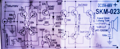
High Power Amplifier
This circuit of power amplifiers using a booster 8 sets sanken , the buffer using transistor D400 and B560 as much 2 sets , and to use part of the driver transistor B546/A940 and D401/C2168. And least 20 volts and the voltage to 70 volts maximum with three voltage is +,-,ground. Power Output 2 X 600 Watt with 8 Ohm Impedance.
 |
| Circuit audio amplifier 600 Watt |
 |
| Circuit of PCB so from 2 X 600 watts (looked down) |
 |
| Circuit of PCB (looked upon) |
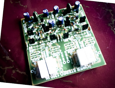 |
| The above is a circuit of ready to operate , just stay put booster. Source : link |
Thursday, April 4, 2013
Symmetric Power Supply Circuit
This is a symmetric power supply that is based on LM7912 IC. There are two IC’s that can used in this circuit. Both of them, is using as voltage regulator and connected with zener diodes to deliver a stable DC voltage. The rectifier and filter is built by rectifier diodes and filter capacitors C1 and C4. Capacitors C2 and C5 is using to stabilize the regulator ICs. This is the figure of the circuit;

The circuit, it becomes unconventional. Both op-amps together with the driver transistors are wired as DC voltage amplifiers. The non-inverting inputs are connected to +2.45 volts through voltage dividers R2/R5 and -2.45 volts through R7/R10. A regulated symmetrical voltage extracted from the voltage divider P1/R1/R9 and subtracted from the fixed +/- 2.45 volts. The negative from IC3 and the positive is from IC4. This results to a symmetrical voltage outputs from +/- 4.9 volts to 18 volts. Capacitors C7 and C8 are stabilizing capacitors. The resistors R6 and R11 are pull-down resistors to preload the outputs in case of an empty load.
The accuracy of the voltage symmetry is dependent on the resistor values of the three voltage divider circuits. If there is non-symmetry in the output, it is probably due to one of the regulator ICs with its 10% tolerance rating. In such case, adding a 5K trimmer in series with R1 or R9 is recommended. Adjust the trimmer until symmetry is achieved.
6 5W audio power amplifier

This amplifier circuit based on the ic, and the use here is that where ic STK4017 IC has output power of 6.5 watts with the impedance 8Ohm. Minimum required supply voltage and maximum 20Volt 35 Volt DC.Component
R1 = 100K
R2 = 2K7
R3 = 27R
C1 = 22uF
C2 = 100uF
C3 = 100uF
C4 = 100uF
C5 = 100uF
C6 = 47uF
C7 = 330uF
C8 = 100uF
U1 = STK4017
Besides using STK4017 ic, ic and can use that I mentioned the following:
STK4019
STK4021
STK4023
STK4025
Tuesday, April 2, 2013
5000 Watts High Power Amplifier Schematic
Circuit Skema Rangkaian - High Power Amplifier has great advantages are 5000W ultra-light, high-power audio amplifier, without switching-mode power supply. This ambit is of an 2 x 2,500W RMS Stereo amplifier, super-light and after switching-mode ability supply. The ambit aloof shows a channel, and the ability accumulation that it assists to the two channels. The audio ambit should be duplicated, but the ability accumulation assists to the two channels after problems.
 |
| Circuit Skema Rangkaian Power Amplifier 5000W |
A adapted affliction should be destined to the careful agent of the audio line, that should be of audio-high-quality, of the blazon acclimated in microphone pre amps ascribe line. The accomplished accumulation (2 channels) of 5,000W RMS it should not counterbalance added than 32 lbs, already central of an adapted brownish box.
WARNING:
This ambit is alone for abecedarian use. It contains not-isolated genitalia of the electric AC net and it can be actual dangerous. The access for the speakers are not abandoned of the calm AC net and it requests added care. This action seeks to acting a accepted ability accumulation with abundant weight and amount reduction, after necessarily to use a switching-mode ability supply.
This action cannot be accustomed in some countries for commercial-use. The columnist doesn’t accept any albatross for the anatomy as that ambit it will be applied.
> Related High Power Amplifier
>> 2800W High Power Amplifier Circuit
>>> 3000W Stereo Power Amplifier
>>>> 1500W HiFi Power Amplifier Circuit
Subscribe to:
Posts (Atom)