Showing posts with label to. Show all posts

Tuesday, February 4, 2014

Simple Voltage to Current Converter Drives White LEDs

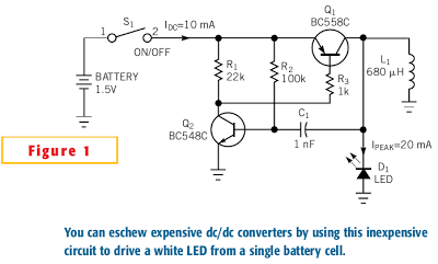
You sometimes need to drive a white LED from one 1.5V battery. Unfortunately, the forward voltage of a white LED is 3 to 4V. So, you would need a dc/dc converter to drive the LED from one battery. Using the simple circuit in Figure 1, you can drive one white LED or two series-connected green LEDs, using only a few components. The circuit is a voltage-to-current converter, which converts the battery voltage to a current that passes through the LED.

You can adjust this current and, thus, the brightness of the LED, by varying resistor R3. If you turn on switch S1, resistor R2 feeds base current to transistor Q2. Q2 turns on, and its collector current, via R3, turns on Q1. Now, the current through inductor L1 increases. The slope of the increase is a function of the value of L1 and the battery voltage. The current through L1 increases until it reaches a maximum value, which depends on the gain of Q1. Because the value of R3 sets the base current drawn from Q1, Q1s collector current is also limited.


White LEDs Circuit Diagram

White LEDs Circuit Diagram


Once the current through L1 reaches its maximum value, the slope of the current through L1 changes. At that instant, the voltage on L1 switches to a negative polarity forced by the changed slope. This negative voltage traverses capacitor C1 and turns off Q2, which in turn turns off Q1. The negative voltage on L1 increases until it reaches the forward voltage of the LED. The peak current through inductor L1 now flows through the LED and decreases to zero. Now, Q2 switches on again, via the current through R2, and the cycle starts again.

By adjusting resistor R3, you can set the peak current through L1 and the peak current through the LED. The brightness of an LED is a linear function of the current through the LED. So, adjusting the value of R3 also adjusts the brightness of the LED.

It doesnt matter which LED you use; the forward voltage on the LED always increases until the peak current through L1 flows through the LED. Different forward voltages of the LEDs yield different on-times (duty cycles) but the same peak current through the LED. With the values shown in Figure 1, the circuit oscillates at a frequency of approximately 30 kHz and delivers a 20-mA peak current through the LED.

The duty cycle depends on the ratio of the battery voltage to the forward voltage of the LED. One advantage of this circuit is that it requires no series-limiting resistor for the LED. The peak current through the LED is a function of the value of R3 and the gain of Q1.[via]
Continue reading...

Wednesday, December 25, 2013

There is no need to get the special training to operate phone jammer

There is no need to get the special training to operate phone jammer .
"Fixed position" be changed to the upper left corner "point X coordinate into a 63" fixed point Y coordinate into a 156 "maximum width" be changed to 102, the frame color, "within the box color, Background color changed to white FFFFFF text color changed to red FF00FF. Set show the effect will be much better. TXT, text is one of the most commonly used text format in the computer, if you want to read and edit the TXT text install YEdit software on the phone. It has a very strong TXT text reading and editing features. After installation, conduct basic settings: Options - Tools - Settings "will open the file encoding to save the file encoding is set for the GB2312, word wrap is set to open. The technical personnel is doing every effort to make phone jammer more effective.
Can now press the "Options - File - New open save the TXT text to open the text, press the" Options - Edit the text to paste Select Find the use of the office suite Quickoffice. 60 version of the Quickoffice the Premier Series is the only one who can edit Microsoft Office documents smartcell phone software on Symbian smartcell phone platform. computer-formatted e-mail attachments directly on the cell phone view and edit additional conversion without the need to do on the computer, and special editorial protection mechanism can keep the original contents of the file. Q: How do I enter Quickword edit mode? To enter edit mode, select "Options - Edit mode so you can directly edit the Quickword document. If there are too many sets of phone jammer , especially after many buildings in the prison implement shielding, it is harder to switch on or off centrally or uniformly.
The Quickword an error when I try to open a Microsoft Word document "doc" file, "do not support the contents of the file, what does this mean? This file have any questions? This situation mostly because trying to open doc file, in fact, RTF (Rich Text Format) files. You can open this file on the computer using Word and then save as DOC format, so that you can successfully open. Note that: similar Wordperfect this program to create the *. Doc file, the actual Rich Text Format (RTF) file. How do I enter punctuation marks? Use the cell phone keypad to enter punctuation, press the "*" key, and then select from the list. Host of phone jammer is installed on the top inside the case.The open meeting of phone jammer review was successfully held in the meeting room
How do I enter a carriage return line feed in the Quickword? You can find the carriage return symbols in the punctuation table. I want to how to highlight text in the Quickword? To highlight text, you must first enter the edit mode, then press the T-shaped key, and drag the joystick, you can highlight text. The Quickword in the clipboard text word limit? There is no limit (depending on the size of the cell phone memory). Menu, select "scan range" mean? This means that you can specify in the cell phone scanned files location.
Continue reading...

Monday, December 23, 2013

A network is rolled out according to a network plan

 A network is rolled out according to a network plan. Services for arias are planned for and provided according to the potential

market. The network operator is a business with shareholders all demanding the best dividends on their investments. A BTS to provide these services to the end user will not be erected for one or

two farmers with the potential to generate R6000pm calls/smss made by themselves and their workers.The leather cases, covers, skins and

belt clips can help you to add a personal touch and amplify the charm of your mobile phone.
Antenna boosters can help you to enjoy the best network connectivity even if you are present in any "Dead Zone". I am sure that you will adore the benefits which are provided by this mobile phone

accessory. You can invest your funds and grab some antenna boosters which can match the personality of your handset. I am sure that you will fall in love with the tempting replicas of these

trimmings.
There are countless online websites which can offer you the accurate information about these mobile phone accessories. You can also grab some matching and obliging mobile phone accessories which

can help you to amplify the utility of your handset. The discount offers which are provided by these sites can help you to enjoy the facilities without any deep-rooted affect on your side-pockets.

I hope that you will enjoy the benefits of these trimmings. The HTC HD2 is the first Windows Mobile with a capacitive touchscreen and also with HTCs Sense UI. The homescreen comes with 13 tabs --

whose icons are depicted at the bottom -- in the form of a dock. These tabs can be customised to the extent that the features can be deactivated but new ones cannot be added. Under the home tab is

the calendar, clock and weather information. Sliding the homescreen up reveals the tabs to add 15 favourite features for direct access. The browser tabs let you add 10 bookmarks. The screen lock is

sliding at the top of the screen and also depicts the number of unnoticed events in the phone like missed calls, unread messages, etc. The main menu of the device is typical of Windows Mobile 6.5

with a honeycomb structure. Contacts can be integrated in a manner similar to previous HTC devices with Sense UI. They can also be integrated with Facebook. The device has a smart dialler, which

finds contacts by dialling the number or name of the contacts. Input options include phone keypad, compact QWERTY and full QWERTY.
Continue reading...

Saturday, September 28, 2013

Stereo to Mono Converter Based on FET

High quality portable unit, Suitable for Subwoofer amplifiers

This simple circuit mixes two or more channels into one channel (e.g. stereo into mono). The circuit can mix as many or as few channels as you like and consume very little power. The mixer is shown with two inputs, but you can add as many as you want by just duplicating the "input sections" which are clearly visible on the schematic.

Circuit Diagram:

Stereo_to_Mono_Converter_Based_on_FETStereo to Mono Converter Based on FET

Parts:

P1 = 10K-50K Pot
P2 = 10K-50K Pot
R1 = 100K
R2 = 100K
R3 = 6.8K
C1 = 0.1uF-25V
C2 = 0.1uF-25V
C3 = 0.1uF-25V
Q1 = 2N3819 Junction FET
J1 = Audio input sockets
J2 = Audio input sockets

Notes:

  • As many or as few channels as are required can be added to the mixer.
  • Do this by just duplicating the input "sections" which are clearly shown on the schematic.
  • One version of this mixer I saw had 18 inputs!
  • A shielded case is probably needed to reduce hum and help stop oscillations.
  • P1 and P2 are dual gang potentiometer for stereo version.
  • The circuit can be powered by a single 9 volt battery.

Source : www.uashem.com

Continue reading...

Tuesday, September 10, 2013

12V to 20V Automotive Power Converter

 12V to +-20V Automotive Power Converter Diagram

12V to +-20V Automotive Power Converter (for audio amplifier)

The limitation of car supply voltage (12V) forces to convert the voltages to higher in order to power audio amplifiers. In fact the max audio power x speaker (with 4 ohm impedance) using 12V is (Vsupply+ - Vsupply-)^2/(8*impedance) 12^2/32 = 4.5Watts per channel, that is laughable... For powering correctly an amplifier the best is to use a symmetric supply with a high voltage differential. for example +20 - -20 = 40Volts in fact 40^2/32 = 50 Watts per channel that is respectable. This supply is intended for two channels with 50W max each (of course it depends on the amplifier used). Though it can be easily scaled up or the voltages changed to obtain different values.
Continue reading...

Monday, May 27, 2013

How to Make an Inductive Li Ion Battery Charger Circuit


Any electrical system which involves wire networks or cables can be very messy and cumbersome. Today the world is getting hi-tech and the electrical systems are also transiting into better and hassle free versions for providing more convenience to us. Inductive power transfer is one such interesting concept which facilitates power transfer without the use of wires, or rather wirelessly. Charging batteries through inductive charging is one of the applications that’s becoming very popular and getting appreciated by the uses. Here we’ll study the concept and one example circuit diagram related to the subject.


As the name refers to, inductive power transfer is a process through which a certain magnitude of power is transferred from one fixed place to another through the air without using conductors, just as radio signals or cell phone signals are transmitted.

However the concept isn’t that easy as it sounds to be, because with radios and cell phones the transmitted power is merely in few watts and thus becomes quite feasible, but transferring  power (wirelessly) so that it can be used for powering high current devices is entirely a different ball game.

 Here we are talking about several watts or probably several hundreds of watts that needs to be carried without any dissipation, from point to the other without using wires, an issue difficult to implement.

However researchers are trying their best to find appropriate set ups which may become just suitable for implementing the above concept successfully.

The following points outline the concept, and help us to know how the above procedure actually takes place:

Induction as we all know is a process through which electrical power is transferred from one position to the other without incorporating direct connections. The best example is our regular electrical transformers, where an input AC is applied at one of its windings and an induced power is received at the other winding through magnetic inductions.

However the distance between the two windings inside a transformer is very small and therefore the actions take place very conveniently and efficiently. When the procedure needs to be implemented at greater distances the task gets a bit complicated.

By evaluating the induction concept we find that there are basically two obstacles that make the power transfer difficult and inefficient, especially as the distance between the inducting destinations are increased.

The first hurdle is the frequency and the second hurdle is the generated eddy currents in the winding core. 

The two parameters are inversely proportionate and therefore are directly dependant on each other. Another factor that hampers the proceedings, is the winding core material, which in turn directly affects the above two parameters.

  By carefully dimensioning these factors in the most efficient way, the distance between the inducting devices can be considerably stretched.

For transferring power in the above discussed method, we firstly require an AC, meaning the power which needs to be transferred must be a pulsating current. This frequency of the current when applied to a winding generates eddy currents, which are reverse currents opposing the applied current.

Generation of more eddy current means less efficiency and more power loss through core heating. However as the frequency is increased, generation of eddy currents is reduced proportionately. 

Also, if a ferrite material is used in place of the conventional iron stampings as the core of the winding helps to further reduce the eddy currents.

Therefore for implanting the above concept in the most efficient way we need to make the source power high in frequency, in the order of many kilohertz and use an input induction system that’s made up of ferrite as the core. Hopefully, this solves the issue to great extents; at least for the making the proposed project of an inductive charging circuit for Li-ion batteries.

About the Circuit

WARNING - THE CIRCUIT IS NOT ISOLATED FROM AC MAINS AND SO IS EXTREMELY DANGEROUS IF TOUCHED IN POWERED CONDITION.

The circuit is devised by me, but has not been verified practically, so I would advise the readers to take a note of this. The circuit can be understood with the following points:

Referring to the figure we see two units, one is the base or the transmitting module and the other one is the receiver module.


As discussed in the above paragraph, the core material of the base winding is a ferrite E-core which is relatively larger in size.

The bobbin that’s fitted inside the E-core has a single stage, neatly wound with 100 turns of 24 SWG super enameled copper wire. A center tap is extracted from the winding from its 50th winding turn.

The above coil or transformer is connected to an oscillator circuit consisting of the transistor T1, preset P1 and the corresponding resistor and capacitor.

The preset is used for increasing the frequency through the winding up to optimal levels and needs to be experimented some.

A DC voltage is fed to the circuit for initiating the required oscillations, which is derived directly by rectifying and filtering the AC mains.

On applying the DC, the circuit begins oscillating and the oscillations from the inductor being high in frequency escapes into the air to a considerable distance and needs to be grabbed back for the proposed inductive reception.

The receiving unit also incorporates an inductor consisting of air cored 50 turns of 21 SWG super enameled copper wire, which becomes a kind of antenna for anticipating the released power waves from the base circuit.

Capacitor C3 is a variable capacitor, the one used in radio for tuning may be tried. Its used for trimming the reception until the resonating point is reached and L2 gets optimally tuned with the transmitting waves.

This instantly raises the output voltage from L2 and becomes optimally suitable for the charging requirements.

D6 and C4 are the rectifying components which finally converts the AC signals into pure DC.

When brought to a considerable proximity, the inductions from the lower base unit is induced inside the receiving coil, the induced frequency is suitably rectified and filtered inside the receiver circuit and is used for charging the connected Li-Ion battery.

CAUTION: THE WHOLE IDEA IS BASED ON MY ASSUMPTIONS ONLY; READERS DISCRETION IS STRICTLY ADVISED WHILE EMPLOYING THE DISCUSSED CONCEPT AND THE CIRCUIT.


Parts List

The following parts would be required for making this inductive battery charging circuit:

R1 = 470 Ohms,
R2 = 10K, 1Watt,
C1 = 0.47uF/400V, non polar,
C2 = 2uF/400V, non polar
C3 = Variable Gang Condenser,
C4 = 10uF/50V,
D1---D5= 1N4007,
D6 = Equal to Battery voltage, 1watt
T1 = UTC BU508 AFI
L1 = 100 turns, 25 SWG, center tap, over largest possible ferrite E-core
L2 = 50 piled turns, 20 SWG, 2 inches diameter, air cored


Continue reading...

Monday, May 13, 2013

Simple Analog to Digital Converter

http://www.electronic-circuits-diagrams.com/computersimages/2.gif


Normally analogue-to-digital con-verter (ADC) needs interfacing through a microprocessor to convert analogue data into digital format. This requires hardware and necessary software, resulting in increased complexity and hence the total cost.
The circuit of A-to-D converter shown here is configured around ADC 0808, avoiding the use of a microprocessor. The ADC 0808 is an 8-bit A-to-D converter, having data lines D0-D7. It works on the principle of successive approximation. It has a total of eight analogue input channels, out of which any one can be selected using address lines A, B and C. Here, in this case, input channel IN0 is selected by grounding A, B and C address lines.Usually the control signals EOC (end of conversion), SC (start conversion), ALE (address latch enable) and OE (output enable) are interfaced by means of a microprocessor. However, the circuit shown here is built to operate in its continuous mode without using any microprocessor. Therefore the input control signals ALE and OE, being active-high, are tied to Vcc (+5 volts).

The input control signal SC, being active-low, initiates start of conversion at falling edge of the pulse, whereas the output signal EOC becomes high after completion of digitisation. This EOC output is coupled to SC input, where falling edge of EOC output acts as SC input to direct the ADC to start the conversion.
As the conversion starts, EOC signal goes high. At next clock pulse EOC output again goes low, and hence SC is enabled to start the next conversion. Thus, it provides continuous 8-bit digital output corresponding to instantaneous value of analogue input. The maximum level of analogue input voltage should be appropriately scaled down below positive reference (+5V) level.The ADC 0808 IC requires clock signal of typically 550 kHz, which can be easily derived from an astable multivibrator constructed using 7404 inverter gates. In order to visualise the digital output, the row of eight LEDs (LED1 through LED8) have been used, wherein each LED is connected to respective data lines D0 through D7. Since ADC works in the continuous mode, it displays digital output as soon as analogue input is applied. The decimal equivalent digital output value D for a given analogue input voltage Vin can be calculated from the relationship
Continue reading...

Tuesday, April 9, 2013

A Simple 5 KVA to 10 KVA Automatic Voltage Stabilizer Circuit Explained 220 Volts 120 Volts

The diagram shows a rather simple voltage stabilizer design which can hold huge output power in the order of 5 to 10KVA. The use of SSR or solid state relays makes the output stage easy to configure and very accurate - thanks to the modern SSRs which are designed to trigger massive power in response to smaller input DC potentials.

The circuit is pretty simple to understand. All the opamps are arranged in standard voltage comparator modes.
The presets P1 to P7 can be adjusted as per the required tripping points, which will correspond to the output SSR switching and the subsequent transformer tap selections.The central green TAP is the normal voltage output, the lower TAPs gradually produce higher voltages while the upper TAPs are set for lower voltages.

These TAPs are chosen by the appropriate SSRs in response to the varying AC voltages, thus adjusting the output voltage to the appliances close to normal levels.This circuit was asked by Mr. Alexandar and the SSR data was provided by him.

Parts List

R1 to R9 = 1K, 1/4 watt,

P1 to P7 = 10K preset,

C1 = 1000uF/25V

VR1 = 1K Preset,

opamps = IC 324,

Transformer = Input 230volts or 120volts, Taps - incrementing/decrementing voltage levels (TAPs) as per individual specs.

SSR = 10KVA/230volts = output, 5 to 32 volts DC = input

COMPLETE SSR SPECIFICATION CAN BE FOUND HERE:

http://www.unisoncontrols.com/ssr-dc-to-ac-1ph.php


Continue reading...

Saturday, April 6, 2013

1 3V DC to 12 2V DC Regulator Power Supply

Power supply circuit to generate output below were variations between 1.3V DC to 12.2V DC with 1A current.
In addition, the power supply circuit is also equipped with over-current protection or shield against belebih flow. Power supply circuit is very simple, but the quality is quite good, made her basiskan regulator IC LM723 is a pretty legendary.


1.3V DC to 12.2V DC Regulator Power Supply

Description:
R2 to set the output voltage. The maximum current is determined by R3, over-current protection circuit inside the LM723 to detect the voltage on R3, if it reaches 0.65 V, the voltage output will be off her. So the current through R3 can not exceed 0.65 / R3 although output short-circuit in his.

C3 and C4 are ceramic capacitors, as much as possible directly soldered to the PCB, this is because the LM723 is prone to oscillation that is not cool.

LM723 works with 9.5V input voltage to 40 V DC and the LM723 can generate its own current of 150mA when the output voltage is not more than 6-7V under input voltage.

Specifications:
Output (value estimated):

Vmin = (R4 + R5) / (R5 * 1.3)
Vmax = (7.15 / R5) * (R4 + R5)

Imax = 0.65/R3

Max. Power on R3: 0.42/R3

Min. DC Input Voltage (pin 12 to pin 7): Vmax + 5

Component List:
B1 40V/2.5A
C1 2200uF (3300uF even better)
C2 4.7uF
C3 100nF
C4 1NF
C5 330nF
C6 100uF
Green LED D1
D2 1N4003
F1 0.2A F
F2 2A M
IC1 LM723 (in a DIL14 plastic package)
R1 1k
R2 Pot. 5k
R3 0.56R/2W

R4 3.3k
R5 4.7k
S1 250V/1A
T1 2N3055 on a heatsink 5K / W
TR1 220V/17V/1.5

source [link] 
Continue reading...

Friday, April 5, 2013

Serial To Parallel Converter

This converter may help if just the serial port on a personal computer is free, whereas the printer needs a parallel (Centronics) port. It converts a serial 2400 baud signal into a parallel signal. The TxD line, pin 3, CTS line, pin 8 and the DSR line, pin 6, of the serial port are used - see diagram. The CTS and DSR signals enable handshaking to be implemented. Since the computer needs real RS232 levels, an adaptation from TTL to RS232 is provided in the converter by a MAX232. This is an integrated level converter that transforms the single +5V supply into a symmetrical ±12V one.

Serial To Parallel Converter circuit diagramThe serial-to-parallel conversion is effected by IC1. This is essentially a programmed PIC controller that produces a Centronics compatible signal from a 2400 baud serial signal (eight data bits, no parity, one stop bit). The IC also generates the requisite control signals. If there is a delay on the Centronics port, the RS232 bitstream from the computer may be stopped via the Flow signal (pin 17). This ensures that no data is lost. The controller needs a 4 MHz ceramic resonator, X1.
Continue reading...

Thursday, April 4, 2013

How to Make a simplest Automatic Battery Charger Circuit Using Just a Single Relay

Amazed to hear this! Yep that’s actually possible, you would need only one relay and a handful of diodes to make a simplest one relay automatic battery charger circuit.

The idea struck me while trying to design the easiest possible battery charger circuit for one my clients.
The concept is simple; just raise the operating or triggering voltage of the relay up to the optimal battery charging threshold voltage by dropping the required amount of supply voltage to the relay coil, with the help of series diodes.
The idea may be understood from the following points:
Take an ordinary relay, measure its triggering voltage by carefully applying a variable voltage across its coil.
Now suppose the triggering voltage of the particular relay was about 9 volts, and also assume you want to raise its voltage to 14 volts, which may be your 12 volt battery’s charging threshold voltage.
We know that a 1N4007 diode drops about 0.6 volts across it, so if we add sufficient number of diodes in series with the relay coil would hopefully pull its tripping or triggering voltage to about 14 volts.
That means, 14 – 9 = 5, we’ll require 5/0.5 = 10 diodes in series to achieve this rise in the triggering voltage of the relay.
That’s pretty simple and interesting isn’t it?
The rest may be done with the help of the shown diagram…..your simplest single relay automatic battery charger is ready. 


Continue reading...

Tuesday, April 2, 2013

5V to 12V Boost Converter Using LT1370

This is a design for booster converter. This booster can convert the voltage from 5 V to 12 V. This circuit is using LT1370 IC as main control. The high 6A switch rating permits the circuit to deliver up to 24W. This is the figure of the circuit.


The inductor needs to be chosen carefully to meet peak current values. The output capacitor can see high ripple currents often, as in this application, higher than the ripple rating of a single capacitor. This requires the use of two surfaces mount tantalums in parallel; both capacitors should be of the same value and manufacturer. The input capacitor does not have to endure such high ripple currents and a single capacitor will normally suffice. The catch diode, D1, must be rated for the output voltage and average output current. The compensation capacitor, C2, normally forms a pole in the 2Hz to 20Hz range, with a series resistor, R3, to add a zero at 1kHz to 5kHz. The S/S pin in this example is driven by a logical on/off signal, a low input forcing the LT1370 into its 12mA shutdown mode.
Continue reading...

12V to 220V converter circuit

This DIY 12V to 220V voltage converter is build with CMOS 4047 that is the main component of this small voltage converter that transforms a 12V DC into 220V AC. 4047 is used as a astable mutivibrator, at pins 10 and 11 will have a symmetrical rectangular signal wich is amplified b 2 Darlington transistors and finally reach the secondary coil of mains transformer ( 2x10V / 60VA ).

At the main voltage converter transformer terminals it will be 220V. With the help of P1 the output frequency can be adjusted between 50Hz to 400Hz. Although this is not part of any professional dc ac converters it can be used quite effective on some home appliances.
For more DC to AC voltage converters check the related posts.


Check out the tags for more 12 Volts to 220 Volts converters.

source [link] 
Continue reading...

Monday, April 1, 2013

Inductorless 3 to 5 Volts Converter

By configuring a comparator and a transistor to control the oscillator in a charge pump circuit, you enable the pump to generate a regulated output of in principle any desired value. Charge pump ICs can either invert or double an input voltage (for example, 3 V to –3 V or 3 V to 6 V). The charge pump itself does not regulate the output voltage and one running off 3 V is not normally capable of generating intermediate output voltage levels like 5 V. However, by adding a comparator and a reference device, you can create arbitrary output levels like 5 V and regulate them as well.
Circuit diagram  :
Inductorless 3-to-5 Volts Converter
Inductorless 3-to-5 Volts Converter Circuit Diagram

Charge pump IC1 (a MAX660) has an internal oscillator whose 45 kHz operation transfers charge from C1 to C2, causing the regulated output to rise.

When the feedback voltage (pin 3 of IC2) exceeds 1.18 V, the output of comparator IC2 (a MAX921) goes high, turning off the oscillator via T1. The comparator hysteresis (easily added on IC2) is zero here simply because no hysteresis is required in the control loop. The oscillator when enabled generates two cycles, which is sufficient to drive VOUT slightly above the desired level. Next, the feedback turns the oscillator off again.
The resulting output ripple will depend mainly on the input voltage and the output load current. Output ripple may be reduced at the expense of circuit efficiency by adding a small resistor (say, 1 ?) in series with C1. You’ll find that ripple also depends on the value and ESR associated with C1 - smaller values of C1 transfer less charge to C2, producing smaller jumps in V OUT.

Continue reading...