Showing posts with label voltage. Show all posts
Showing posts with label voltage. Show all posts
Tuesday, February 4, 2014
Simple Voltage to Current Converter Drives White LEDs
You sometimes need to drive a white LED from one 1.5V battery. Unfortunately, the forward voltage of a white LED is 3 to 4V. So, you would need a dc/dc converter to drive the LED from one battery. Using the simple circuit in Figure 1, you can drive one white LED or two series-connected green LEDs, using only a few components. The circuit is a voltage-to-current converter, which converts the battery voltage to a current that passes through the LED.
You can adjust this current and, thus, the brightness of the LED, by varying resistor R3. If you turn on switch S1, resistor R2 feeds base current to transistor Q2. Q2 turns on, and its collector current, via R3, turns on Q1. Now, the current through inductor L1 increases. The slope of the increase is a function of the value of L1 and the battery voltage. The current through L1 increases until it reaches a maximum value, which depends on the gain of Q1. Because the value of R3 sets the base current drawn from Q1, Q1s collector current is also limited.
White LEDs Circuit Diagram
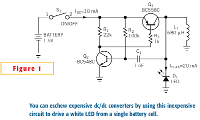
Once the current through L1 reaches its maximum value, the slope of the current through L1 changes. At that instant, the voltage on L1 switches to a negative polarity forced by the changed slope. This negative voltage traverses capacitor C1 and turns off Q2, which in turn turns off Q1. The negative voltage on L1 increases until it reaches the forward voltage of the LED. The peak current through inductor L1 now flows through the LED and decreases to zero. Now, Q2 switches on again, via the current through R2, and the cycle starts again.
By adjusting resistor R3, you can set the peak current through L1 and the peak current through the LED. The brightness of an LED is a linear function of the current through the LED. So, adjusting the value of R3 also adjusts the brightness of the LED.
It doesnt matter which LED you use; the forward voltage on the LED always increases until the peak current through L1 flows through the LED. Different forward voltages of the LEDs yield different on-times (duty cycles) but the same peak current through the LED. With the values shown in Figure 1, the circuit oscillates at a frequency of approximately 30 kHz and delivers a 20-mA peak current through the LED.
The duty cycle depends on the ratio of the battery voltage to the forward voltage of the LED. One advantage of this circuit is that it requires no series-limiting resistor for the LED. The peak current through the LED is a function of the value of R3 and the gain of Q1.[via]
Continue reading...
You can adjust this current and, thus, the brightness of the LED, by varying resistor R3. If you turn on switch S1, resistor R2 feeds base current to transistor Q2. Q2 turns on, and its collector current, via R3, turns on Q1. Now, the current through inductor L1 increases. The slope of the increase is a function of the value of L1 and the battery voltage. The current through L1 increases until it reaches a maximum value, which depends on the gain of Q1. Because the value of R3 sets the base current drawn from Q1, Q1s collector current is also limited.
White LEDs Circuit Diagram
Once the current through L1 reaches its maximum value, the slope of the current through L1 changes. At that instant, the voltage on L1 switches to a negative polarity forced by the changed slope. This negative voltage traverses capacitor C1 and turns off Q2, which in turn turns off Q1. The negative voltage on L1 increases until it reaches the forward voltage of the LED. The peak current through inductor L1 now flows through the LED and decreases to zero. Now, Q2 switches on again, via the current through R2, and the cycle starts again.
By adjusting resistor R3, you can set the peak current through L1 and the peak current through the LED. The brightness of an LED is a linear function of the current through the LED. So, adjusting the value of R3 also adjusts the brightness of the LED.
It doesnt matter which LED you use; the forward voltage on the LED always increases until the peak current through L1 flows through the LED. Different forward voltages of the LEDs yield different on-times (duty cycles) but the same peak current through the LED. With the values shown in Figure 1, the circuit oscillates at a frequency of approximately 30 kHz and delivers a 20-mA peak current through the LED.
The duty cycle depends on the ratio of the battery voltage to the forward voltage of the LED. One advantage of this circuit is that it requires no series-limiting resistor for the LED. The peak current through the LED is a function of the value of R3 and the gain of Q1.[via]

Tuesday, December 24, 2013
Build a High voltage Bucking Regulator Circuit Diagram
This High voltage Bucking Regulator Circuit Diagram is basically tbe classic bucking regulator, except it uses a TMOS N-channel power FET for the chopper and creates its own supply for the gate control. Tht unique aspect of this circuit is how it generates a separate supply for the gate circuit, which must be greater than Vvv.
When power is applied, C2 charges, through D2, to +12 V. At this time, Q1 is off and the voltage at point A is just below zero. When the pulse-modulated signal is applied, the optoisolator transistors, Q2 and Q3, supply a signal to Q1 that turns it on. The voltage at point A then goes to Vvn. C2 back-biases D2, and the voltage at point B becomes 12 V above Vnn· After Q1 is turned on, current starts to flow through L1 into C1, increasing until Q1 turns off.
High voltage Bucking Regulator Circuit Diagram

The current still wants to flow through Ll, so the voltage at point A moves toward negative infinity, but is clamped by D1 to just below zero. Current flows less and less into C1, until Q1 turns on again. Q2 and Q3 drive Q1 `s gate between the voltages at point A and B, which is always a12 V swing, so Vcs max. is never exceeded. For proper operation, the 12-V supply has to be established before the pulse-width modulator signal is applied.
Saturday, December 21, 2013
Build a High Voltage Dc Generator Circuit Diagram
High Voltage Dc Generator Circuit Diagram. In the miniature high-voltage dc generator, the input to the circuit, taken from a 12-Vdc power supply, is magnified to provide a 10,000-Vdc output causing a pulsating signal, of opposite polarity, to be induced in Tl`s secondary winding.
The pulsating dc output at the secondary winding of Tl (ranging from 800 to 1000 V) is applied to a 10-stage voltage-multiplier circuit, which consists of D1 through D10, and C3 through C12. The multiplier circuit increased the voltage 10 times, producing an output of up to 10,000 Vdc. The multiplier accomplishes its task by charging the capacitors (C3 tlirough C12); the output is a series addition of the voltages on all the capacitors in the multiplier. In order for the circuit to operate efficiently, the frequency of the square wave, and therefore the signal applied to the multiplier, must be considered.
The output frequency of the oscillator (Ul-a) is set by the combined values of Kv Rr>, and C{ (which with the values specified is approximately 15 kHz). Potentiometer R5 is used to fine tune the output frequency of the oscillator. The higher the frequency of the oscillator, the lower the capacitivc reactance in the multiplier. Light-emitting diode LED1 serves as an input-power indicator, and neon lamp NE1 indicates an output at the secondary of Tl. A good way to get the maximum output at the multiplier is to connect an oscilloscope to the high-voltage output of the multiplier, via a high-voltage probe, and adjust potentiometer R5 for the maximum voltage output.
High Voltage Dc Generator Circuit Diagram

Wednesday, October 9, 2013
Over Voltage Protection
When a sensitive circuit must under no circumstances have too high a supply voltage applied, then some means of disconnecting the supply must be provided. One way to achieve this is to trigger a thyristor to blow a fuse. A less destructive alternative possibility is to use a MOSFET to disconnect the supply. An over-voltage protection IC, the LTC1696 from Linear Technology (www.linear-tech.com), has recently become available, which is suitable for triggering and driving such a device. It operates from a power supply in the range 2.7 V to 27 V and can be connected to the unregulated input of a voltage regulator. Two voltages can be monitored using feedback pins FB1 and FB2, suitably divided down using potential dividers.
 The trigger threshold for both FB1 and FB2 is +0.88V. The value of the upper resistor in the potential divider can be calculated using the following formula: R1 = 33 kΩ× [(VLIMIT – 0.88 V)/0.88 V] The value of the capacitor connected to the TIMER/RESET pin sets the delay before the protection is triggered. The charging current for this capacitor depends non-linearly on the amount by which the voltage exceeds the threshold value. The greater the over-voltage, the faster the IC triggers. Once triggered the IC remains in that state until either the input voltage is removed or the internal latch is cleared using the MOSFET connected to the TIMER/RESET input.
Continue reading...
 The trigger threshold for both FB1 and FB2 is +0.88V. The value of the upper resistor in the potential divider can be calculated using the following formula: R1 = 33 kΩ× [(VLIMIT – 0.88 V)/0.88 V] The value of the capacitor connected to the TIMER/RESET pin sets the delay before the protection is triggered. The charging current for this capacitor depends non-linearly on the amount by which the voltage exceeds the threshold value. The greater the over-voltage, the faster the IC triggers. Once triggered the IC remains in that state until either the input voltage is removed or the internal latch is cleared using the MOSFET connected to the TIMER/RESET input.
Tuesday, May 14, 2013
High Low voltage cut off with delay alarm

This straight forward circuit will protect electrical appliances from over voltage as well as under voltage.The circuit also produces an alarm when the power supply comes back.An ideal circuit for home to protect your valuable equipments from voltage fluctuations.The same circuit with some modifications can be used to make a automatic voltage stabilizer
When the mains voltage is in the normal level ,the voltage at the negative terminal of zener diode D4 will be less than 5.6 Volts.At this condition transistor T1 will not conduct.The same time voltage at the negative terminal of zener diode D5 will be greater than 5.6 and so the transistor T2 will be conducting.The relay will be activated and the green LED wil be glowing.
When the mains voltage is higher than the set limit the transistor T1 becomes conducting since the voltage at the negative terminal of D4 is greater than 5.6 V.At the same time transistor T2 will be non conducting which results in the deactivation of relay to cut the mains supply from load.When the mains voltage is less than the set limit transistors T1 & T2 becomes non conducting making the relay to de- activate and cut the load from mains.Ω
The timer NE555 is wired as a monostable multivibrator with a pulse width of 10ms.When the power comes back after a cut off a negative voltage is obtained at the trigger pin which triggers the IC NE555.The transistor T3 gets forward biased and it drives the buzzer to produce a beep as an indication of power resumption.Also the transistor T1 is made on which in turn makes T2 off.As a result the relay will remain de- activate for 10ms and this provides the sufficient delay and the equipment is protected from surge voltages.
* To calibrate the circuit a autotransformer is needed.Connect the output of autotransformer to the transformer primary.
* Set the voltage to 260V and adjust VR1 to make the relay deactivated.
* Now set the autotransformer to 160V and adjust VR2 so that the relay is de-energized.
* VR3 can be used to vary the volume of buzzer.
Tuesday, April 9, 2013
A Simple 5 KVA to 10 KVA Automatic Voltage Stabilizer Circuit Explained 220 Volts 120 Volts
The diagram shows a rather simple voltage stabilizer design which can hold huge output power in the order of 5 to 10KVA. The use of SSR or solid state relays makes the output stage easy to configure and very accurate - thanks to the modern SSRs which are designed to trigger massive power in response to smaller input DC potentials.
The circuit is pretty simple to understand. All the opamps are arranged in standard voltage comparator modes.
The presets P1 to P7 can be adjusted as per the required tripping points, which will correspond to the output SSR switching and the subsequent transformer tap selections.The central green TAP is the normal voltage output, the lower TAPs gradually produce higher voltages while the upper TAPs are set for lower voltages.
These TAPs are chosen by the appropriate SSRs in response to the varying AC voltages, thus adjusting the output voltage to the appliances close to normal levels.This circuit was asked by Mr. Alexandar and the SSR data was provided by him.
Parts List
R1 to R9 = 1K, 1/4 watt,
P1 to P7 = 10K preset,
C1 = 1000uF/25V
VR1 = 1K Preset,
opamps = IC 324,
Transformer = Input 230volts or 120volts, Taps - incrementing/decrementing voltage levels (TAPs) as per individual specs.
SSR = 10KVA/230volts = output, 5 to 32 volts DC = input
COMPLETE SSR SPECIFICATION CAN BE FOUND HERE:
http://www.unisoncontrols.com/ssr-dc-to-ac-1ph.php

The circuit is pretty simple to understand. All the opamps are arranged in standard voltage comparator modes.
The presets P1 to P7 can be adjusted as per the required tripping points, which will correspond to the output SSR switching and the subsequent transformer tap selections.The central green TAP is the normal voltage output, the lower TAPs gradually produce higher voltages while the upper TAPs are set for lower voltages.
These TAPs are chosen by the appropriate SSRs in response to the varying AC voltages, thus adjusting the output voltage to the appliances close to normal levels.This circuit was asked by Mr. Alexandar and the SSR data was provided by him.
Parts List
R1 to R9 = 1K, 1/4 watt,
P1 to P7 = 10K preset,
C1 = 1000uF/25V
VR1 = 1K Preset,
opamps = IC 324,
Transformer = Input 230volts or 120volts, Taps - incrementing/decrementing voltage levels (TAPs) as per individual specs.
SSR = 10KVA/230volts = output, 5 to 32 volts DC = input
COMPLETE SSR SPECIFICATION CAN BE FOUND HERE:
http://www.unisoncontrols.com/ssr-dc-to-ac-1ph.php
Subscribe to:
Posts (Atom)