Showing posts with label build. Show all posts
Showing posts with label build. Show all posts
Friday, December 27, 2013
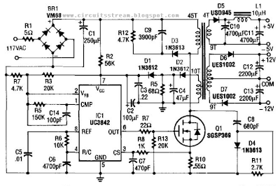
Build a 5v And 12V Ac Powered Switching Supply Circuit Diagram
How to Build a 5v And 12V Ac Powered Switching Supply Circuit Diagram? This supply uses an SGS-Thomson UC3842 IC in an off-line flyback regulator, providing + 5 V at 4 A and ± 12 V at 300 mA. This enables a small high-frequency (50 kHz) transformer, to handle large amounts of power that are normally handled by a 60-Hz transformer.
Q1 is a 5-A 500-V MOSFET, and the diodes are fast-recovery types. T1 has a 45-turn primary winding of #26 wire. The 12-V windings are each 9 turns of #30 wire, bifilar wound. The 5-V winding is 4 turns of four bifilar #26 wires. The control (feedback) winding is two bifilar, parallel 10-turn, #30 windings. The core is Ferroxcube EC35-3C8 with a 3/s` center leg.
5v And 12V Ac Powered Switching Supply Circuit Diagram

Tuesday, December 24, 2013
Build a High voltage Bucking Regulator Circuit Diagram
This High voltage Bucking Regulator Circuit Diagram is basically tbe classic bucking regulator, except it uses a TMOS N-channel power FET for the chopper and creates its own supply for the gate control. Tht unique aspect of this circuit is how it generates a separate supply for the gate circuit, which must be greater than Vvv.
When power is applied, C2 charges, through D2, to +12 V. At this time, Q1 is off and the voltage at point A is just below zero. When the pulse-modulated signal is applied, the optoisolator transistors, Q2 and Q3, supply a signal to Q1 that turns it on. The voltage at point A then goes to Vvn. C2 back-biases D2, and the voltage at point B becomes 12 V above Vnn· After Q1 is turned on, current starts to flow through L1 into C1, increasing until Q1 turns off.
High voltage Bucking Regulator Circuit Diagram

The current still wants to flow through Ll, so the voltage at point A moves toward negative infinity, but is clamped by D1 to just below zero. Current flows less and less into C1, until Q1 turns on again. Q2 and Q3 drive Q1 `s gate between the voltages at point A and B, which is always a12 V swing, so Vcs max. is never exceeded. For proper operation, the 12-V supply has to be established before the pulse-width modulator signal is applied.
Saturday, December 21, 2013
Build a High Voltage Dc Generator Circuit Diagram
High Voltage Dc Generator Circuit Diagram. In the miniature high-voltage dc generator, the input to the circuit, taken from a 12-Vdc power supply, is magnified to provide a 10,000-Vdc output causing a pulsating signal, of opposite polarity, to be induced in Tl`s secondary winding.
The pulsating dc output at the secondary winding of Tl (ranging from 800 to 1000 V) is applied to a 10-stage voltage-multiplier circuit, which consists of D1 through D10, and C3 through C12. The multiplier circuit increased the voltage 10 times, producing an output of up to 10,000 Vdc. The multiplier accomplishes its task by charging the capacitors (C3 tlirough C12); the output is a series addition of the voltages on all the capacitors in the multiplier. In order for the circuit to operate efficiently, the frequency of the square wave, and therefore the signal applied to the multiplier, must be considered.
The output frequency of the oscillator (Ul-a) is set by the combined values of Kv Rr>, and C{ (which with the values specified is approximately 15 kHz). Potentiometer R5 is used to fine tune the output frequency of the oscillator. The higher the frequency of the oscillator, the lower the capacitivc reactance in the multiplier. Light-emitting diode LED1 serves as an input-power indicator, and neon lamp NE1 indicates an output at the secondary of Tl. A good way to get the maximum output at the multiplier is to connect an oscilloscope to the high-voltage output of the multiplier, via a high-voltage probe, and adjust potentiometer R5 for the maximum voltage output.
High Voltage Dc Generator Circuit Diagram

Wednesday, August 14, 2013
Build a Low pass filter Circuit Diagram
This Low-pass filter Circuit Diagram is useful where fast signal acquisition and high precision are required, as in electronic scales. The filters time constant is set by the 2 ohm resistor and the 1 µ capacitor until comparator No. 1 switches. The time constant is then set by the 1.5 ohm resistor and the 1 jtF capacitor. Comparator No. 2 provides a quick reset. The circuit settles to a final value three times as fast as a simple 1.5 ohm—1 µ¥ filter, with almost no dc error.
Low-pass filter Circuit Diagram

Subscribe to:
Posts (Atom)