Showing posts with label amplifier. Show all posts

Sunday, October 6, 2013

Amplifier Timer Circuit Diagram

Turns-off your amplifier when idle for 15 minutes, Fed by amplifier tape-output

This circuit turns-off an amplifier or any other device when a low level audio signal fed to its input is absent for 15 minutes at least. Pushing P1 the device is switched-on feeding any appliance connected to SK1. Input audio signal is boosted and squared by IC2A & IC2B and monitored by LED D4. When D4 illuminates, albeit for a very short peak, IC3 is reset and restarts its counting. Pin 2 of IC3 remains in the low state, the two transistors are on and the relay operates. When, after a 15 minutes delay, no signal appeared at the input, IC3 ends its counting and pin 2 goes high. Q1 & Q2 stop conducting and the relay switches-off. The device is thus completely off as also are the appliances connected to SK1. C5 & R9 reset IC3 at power-on. P2 allows switch-off at any moment.

Parts:

R1,R8___________1K 1/4W Resistors
R2,R3___________4K7 1/4W Resistors
R4_____________22K 1/4W Resistor
R5______________4M7 1/4W Resistor
R6,R9__________10K 1/4W Resistors
R7______________1M5 1/4W Resistor
R10___________100K 1/4W Resistor
R11____________15K 1/4W Resistor
R12____________10M 1/4W Resistor
R13_____________1M 1/4W Resistor
R14_____________8K2 1/4W Resistor
R15_____________1K8 1/4W Resistor
C1____________470µF 25V Electrolytic Capacitor
C2,C3,C6______100nF 63V Polyester Capacitors
C4,C5__________10µF 25V Electrolytic Capacitors
D1_____Diode bridge 100V 1A
D2,D7________1N4002 100V 1A Diodes
D3__________Red LED 5mm.
D4_______Yellow LED 5mm.
D5,D6________1N4148 75V 150mA Diodes
IC1___________78L12 12V 100mA Voltage regulator IC
IC2___________LM358 Low Power Dual Op-amp
IC3____________4060 14 stage ripple counter and oscillator IC
Q1____________BC557 45V 100mA PNP Transistor
Q2____________BC337 45V 800mA NPN Transistor
J1______________RCA audio input socket
P1_____________SPST Mains suited Pushbutton
P2_____________SPST Pushbutton
T1_____________220V Primary, 12V Secondary 3VA Mains transformer
RL1___________10.5V 270 Ohm Relay with SPST 5A 220V switch
PL1____________Male Mains plug
SK1__________Female Mains socket

Notes:
  • Simply connect left or right channel tape output of your amplifier to J1.
  • You can employ two RCA input sockets wired in parallel to allow pick-up audio signals from both stereo channels.
  • The delay time can be varied changing R13 and/or C6 values.
  • Needing to operate a device not supplied by power mains, use a double pole relay switch, connecting the second pole switch in series to the device supply.
Continue reading...

Tuesday, August 6, 2013

170W AMPLIFIER BTL LM4651 LM4652 CIRCUIT DIAGRAM

170W AMPLIFIER BTLLM4651 & LM4652 CIRCUIT DIAGRAM

IC LM4651 is a integrated conventional pulse width modulator driver IC. The IC contains short circuit, under voltage, over modulation, and thermal shut down protection circuitry. The LM4651 also contains a standby function which shuts down the pulse width modulation minimizing supply current.

IC LM4652 is a fully integrated H-bridge power MOSFET IC in a TO-220 power package. The LM4652 has a temperature sensor built in to alert the LM4651 when the die temperature of the LM4652 exceeds the threshold. Together, these two ICs form a simple, compact high power audio amplifier solution complete with protection normally seen only in Class AB amplifiers. Few external components and minimal traces between the ICs keep the PCB area small and aids in EMI control.

Absolute Maximum Ratings LM4651 & LM4652

  • Supply Voltage ± 22V
  • Output Current (LM4652) 10A
  • Power Dissipation (LM4651) 1.5W
  • Power Dissipation (LM4652) 32W
  • ESD Susceptibility (LM4651) 2000V,
  • ESD Susceptibility LM4652 (pins 2,6,10,11) 500V
  • ESD Susceptibility (LM4651) (Note 5) 200V
  • ESD Susceptibility LM4652 (pins 2,6,10,11) 100V
  • Junction Temperature 150°C
  • Soldering Information N, TA and TF Package (10 seconds) 260°C
  • Storage Temperature -40°C to + 150°C
Continue reading...

Wednesday, June 12, 2013

Playback Amplifier For Cassette Deck circuit schematic with explanation

For some time now, there have been a number of tape cassette decks available at low prices from mail order businesses and electronics retailers. Such decks do not contain any electronics, of course. It is not easy to build a recording amplifier and the fairly complex magnetic biasing circuits, but a playback amplifier is not too difficult as the present one shows. The stereo circuits in the diagram, in conjunction with a suitable deck, form a good-quality cassette player. The distortion and frequency range (up to 23 kHz) are up to good standards. Moreover, the circuit can be built on a small board for incorporation with the deck in a suitable enclosure. Both terminals of coupling capacitor C1 are at ground potential when the amplifier is switched on.

Circuit diagram:Cassette Deck Playback Amplifier Circuit Diagram
Cassette Deck Playback Amplifier Circuit Diagram

Because of the symmetrical ±12 V supply lines, the capacitor will not be charged. If a single supply is used, the initial surge when the capacitor is being charged causes a loud click in the loudspeaker and, worse, magnetizes the tape. The playback head provides an audio signal at a level of 200–500 mV. The two amplifiers raise this to line level, not linearly, but in accordance with the RIAA equalization characteristic for tape recorders. Broadly speaking, this characteristic divides the frequency range into three bands:
  • Up to 50 Hz, corresponding to a time constant of 3.18 ms, the signal is highly and linearly amplified.
  • Between 50 Hz and 1.326 kHz, corresponding to a time constant of 120 µs, for normal tape, or 2.274 kHz, corresponding to a time constant of 70 µs, for chromium dioxide tape, the signal is amplified at a steadily decreasing rate.
  • Above 1.326 kHz or 2.274 kHz, as the case may be, the signal is slightly and linearly amplified. This characteristic is determined entirely by A1 (A1’). To make the amplifier suitable for use with chromium dioxide tape, add a double-pole switch (for stereo) to connect a 2.2 kΩ resistor in parallel with R3 (R3’). The output of A1 (A1’) is applied to a passive high-pass rumble filter, C3-R5 (C3’-R5’) with a very low cut-off frequency of 7 Hz. The components of this filter have exactly the same value as the input filter, C1-R1 (C1’-R1’). The second stage, A2 (A2’) amplifies the signal ´100, that is, to line level (1V r.m.s.).
Continue reading...

LM4906 Boomer Audio Power Amplifier circuit and epxlanation

The well-known LM386 is an excellent choice for many designs requiring a small audio power amplifier (1-watt) in a single chip. However, the LM386 requires quite a few external parts including some electrolytic capacitors, which unfortunately add volume and cost to the circuit. National Semiconductor recently introduced its Boomer® audio integrated circuits which were designed specifically to provide high quality audio while requiring a minimum amount of external components (in surface mount packaging only). The LM4906 is capable of delivering 1 watt of continuous average power to an 8-ohm load with less than 1% distortion (THD+N) from a +5 V power supply. The chip happily works with an external PSRR (Power Supply Rejection Ratio) bypass capacitor of just 1 µF minimum.


In addition, no output coupling capacitors or bootstrap capacitors are required which makes the LM4906 ideally suited for cellphone and other low voltage portable applications. The LM4906 features a low-power consumption shutdown mode (the part is enabled by pulling the SD pin high). Additionally, an internal thermal shutdown protection mechanism is provided. The LM4906 also has an internal selectable gain of either 6 dB or 12 dB. A bridge amplifier design has a few distinct advantages over the single-ended configuration, as it provides differential drive to the load, thus doubling output swing for a specified supply voltage. Four times the output power is possible as compared to a single-ended amplifier under the same conditions (particularly when considering the low supply voltage of 5 to 6 volts).

Circuit diagram:
LM4906 Boomer Audio Power Amplifier circuit schematic
Boomer Audio Power Amplifier Circuit Diagram

When pushed for output power, the small SMD case has to be assisted in keeping a cool head. By adding copper foil, the thermal resistance of the application can be reduced from the free air value, resulting in higher PDMAX values without thermal shutdown protection circuitry being activated. Additional copper foil can be added to any of the leads connected to the LM4906. It is especially effective when connected to VDD, GND, and the output pins. A bridge configuration, such as the one used in LM4906, also creates a second advantage over single-ended amplifiers. Since the differential outputs, Vo1 and Vo2, are biased at half-supply, no net DC voltage exists across the load.

This eliminates the need for an output coupling capacitor which is required in a single supply, single-ended amplifier configuration. Large input capacitors are both expensive and space hungry for portable designs. Clearly, a certain sized capacitor is needed to couple in low frequencies without severe attenuation. But in many cases the speakers used in portable systems, whether internal or external, have little ability to reproduce signals below 100 Hz to 150 Hz. Thus, using a large input capacitor may not increase actual system performance. Also, by minimizing the capacitor size based on necessary low frequency response, turn-on pops can be minimized.
Continue reading...

Friday, April 12, 2013

4 X 15 Watt Mini Power Amplifier

A lot of electronic circuits in the domain of audio amplifiers are already been published here. This circuit is a little different because it is a four channel amplifier. Each channel of this amplifier can deliver an output of 15Watts into a 4 ohm speaker. The amplifier can be operated from a single 12V DC supply and this makes it possible to use this amplifier in car audio applications too.

Circuit diagram :
4X15W-amplifier-circuit Diagram
4 X 15 Watt Mini Power Amplifier

The circuit is based on the 15W BTL X 2 channel audio power amplifier IC TA8215 from Toshiba. Even though chip is specifically designed for car audio applications it can be also used for home audio applications. Two TA8215 ICs are used here in order to obtain a 4 channel amplifier system. The circuit is designed almost exactly as per the application diagram in the ICs datasheet. Pins 7 and 19 are the Vcc pins of the ICs internal integrated power amplifier stages and these pins are connected to the positive supply. Pin 9 is the Vcc pin for ICs internal preamplifier and it is also connected to the positive supply. Pins 13 and 14 are the internal power amplifiers ground pins and they are tied together and connected to the ground. 

The internal preamplifier’s ground pin (pin5) is connected to the common ground through a 10 Ohm resistor which makes the input ground separated from the common ground by a resistance of 10 ohms and this improves the noise rejection. The 100uF capacitor works as a power supply de-coupler. The resistor networks connected to the output lines of each amplifier improves the high frequency stability. The variable resistors (R3, R4, R12 and R13) works as the volume controller for the corresponding channels.

Notes :
  • Assembling the circuit on a good quality PCB is a must for obtaining optimum sound quality.
  • Use 12V DC for powering the circuit.
  • The ICs must be fitted with adequately sized heat sinks.
  • R3, R4, R12 and R13 serves as volume controllers.
  • K1 to K4 can be 4 Ohm, 20W speakers.
  • This amplifier circuit can be used in a variety of applications such as car audio systems, home theater systems, personal audio systems, public address systems etc. link
Continue reading...

Hydrophone Booster Amplifier HA2

Hydrophone Booster Amplifier (HA2)
The HP series Hydrophone Booster Amplifier (HA2) amplifies low-level hydrophone signals over a wide range of frequencies. It has a minimum gain of 25dB and an input and output impedance of 50Ω. The HA2 is designed for use with either Precision Acoustics membrane hydrophone or Precision Acoustics HP Series Hydrophone Measurement System, which is shown in Fig 1.
Hydrophone Booster Amplifier
Alternatively, the HA2 may be used when the acoustic signal is provided by a high output impedance hydrophone, such as a GEC-Marconi membrane device, or a conventional hydrophone. In this instance a BNC/MCX adaptor is used which connects directly to the HP Series Submersible Preamplifier, using it as a buffer amplifier, (i.e. the standard Precision Acoustic HP Series configuration shown in Fig 1 is used, but without the interchangeable probe).
The HA2 amplifier is straightforward to use but the following points should be noted:
  • The output of the amplifier should be correctly terminated in 50Ω before operation.
  • The HA2 amplifier is non-inverting but this is of no consequence when used with the HP Series interchangeable probes as their design takes this into account. However when a submersible preamplifier is used as a high impedance buffer amplifier (as in Fig 2) the system output from the HA2 will be inverted as the HP Series Submersible Preamplifier is inverting.
Before Connecting the unit please read WARNING
To Connect
To  Disconnect
1 Connect Output Load 1 Remove RF Input
2 Apply DC Voltage 2 Remove DC Volts
3 Apply RF Input 3 Remove Load

Specification (HA2 Amplifier Only)
Voltage Gain = 25dB minimum
Bandwidth =  50kHz to 125MHz ±1.0dB
Maximum Output Level = 29dBm for 1dB compression (18.1V pk – pk into 50Ω load)
Input Impedance = Nominal 50Ω
Output Impedance  Nominal 50Ω (VSWR 2:1)
Output Noise Level = Typically 70μV pk – pk (bandwidth 125MHz)
Noise Figure = Typically 10dB
Phase = Non-inverting
Terminations:
Front panel = Input BNC socket BNC Output socket
Rear panel Power Requirements = 28v dc output to supply DC Coupler 100/120/220/240V ac, 50 to 60Hz,
7.5W
Operating Temperature = 0 to 50°C
Size = (90mm × 205mm ×194mm)
Weight = 2.6kg


Streampowers
Continue reading...

Thursday, April 11, 2013

Modular Headphone Amplifier

140mW into 32 Ohm loads, Ultra-low Distortion

Those wanting private listening to their music programme should add this Headphone Amplifier to the Modular Preamplifier chain. The circuit was kept as simple as possible compatibly with a High Quality performance. This goal was achieved by using two NE5532 Op-Amps in a circuit where IC1B is the "master" amplifier wired in the common non-inverting configuration already used in the Control Center Line amplifier. IC1A is the "slave" amplifier and is configured as a unity-gain buffer: parallel amplifiers increase output current capability of the circuit. Two Headphone outputs are provided by J3 and J4.

The ac gain of the amplifier was kept deliberately low because this module is intended to be connected after the Control Center module, which provides the gain sufficient to drive the power amplifier. If you intend to use this Headphone Amplifier as a stand-alone device, a higher ac gain could be necessary in order to cope with a CD player or Tuner output. This is accomplished by lowering the value of R1 to 1K5. In this way an ac gain of 9 is obtained, more than sufficient for the purpose. Contrary to the two 15V positive and negative regulator ICs used in other modules of this preamp, two 9V devices were employed instead. This because the NE5532 automatically limits its output voltage into very low loads as 32 Ohm in such a way that the output amplitude of the amplified signal remains the same, either the circuit is powered at ±9V or ±15V. The choice of a ±9V supply allows less power dissipation and better performance of the amplifier close to the clipping point.

The input socket of this amplifier must be connected to the Main Out socket of the Control Center Module. As this output is usually reserved to drive the power amplifier, a second socket (J2) wired in parallel to J1 is provided for this purpose. As with the other modules of this series, each electronic board can be fitted into a standard enclosure: Hammond extruded aluminum cases are well suited to host the boards of this preamp. In particular, the cases sized 16 x 10.3 x 5.3 cm or 22 x 10.3 x 5.3 cm have a very good look when stacked. See below an example of the possible arrangement of the front and rear panels of this module.

Circuit diagram :

Modular Headphone Amplifier Circuit Diagram

Modular Headphone Amplifier Circuit Diagram

Parts:

P1___________47K Log. Potentiometer (twin concentric-spindle dual gang for stereo)
R1___________4K7 1/4W Resistor
R2___________12K 1/4W Resistor
R3,R4________33R 1/4W Resistors
R5,R6________4R7 1/4W Resistors
C1___________1µF 63V Polyester Capacitor
C2,C5________100nF 63V Polyester Capacitors
C3,C6________22µF 25V Electrolytic Capacitors
C4,C7________2200µF 25V Electrolytic Capacitors
IC1__________NE5532 Low noise Dual Op-amp
IC2__________78L09 9V 100mA Positive Regulator IC
IC3__________79L09 9V 100mA Negative Regulator IC
D1,D2_______1N4002 200V 1A Diodes
J1,J2________RCA audio input sockets
J3,J4________6mm. or 3mm. Stereo Jack sockets
J5___________Mini DC Power Socket

Notes:

  • The circuit diagram shows the Left channel only and the power supply.
  • Some parts are in common to both channels and must not be doubled. These parts are: P1 (if a twin concentric-spindle dual gang potentiometer is used), IC2, IC3, C2, C3, C4, C5, C6, C7, D1, D2, J3, J4 and J5.
  • This module requires an external 15 - 18V ac (100mA minimum) Power Supply Adaptor.

Technical data:

Output power (1KHz sinewave):
32 Ohm: 140mW RMS
Sensitivity:
275mV input for 1V RMS output into 32 Ohm load (31mW)
584mV input for 2.12V RMS output into 32 Ohm load (140mW)
Frequency response @ 2V RMS:
Flat from 15Hz to 23KHz
Total harmonic distortion into 32 Ohm load @ 1KHz:
1V RMS and 2V RMS 0.0012%
Total harmonic distortion into 32 Ohm load @ 10KHz:
1V RMS and 2V RMS 0.0008%

Source :  www.redcircuits.com

Continue reading...

56W AUDIO AMPLIFIER IC lm3876 or 3886 CIRCUIT DIAGRAM

56W AUDIO AMPLIFIER IC lm3876 or 3886 CIRCUIT DIAGRAM

Voltage gain is 27dB as shown, but this can be changed by using a different value resistors for the feedback path (R3, currently 22k, between pins 3 and 9). The inductor consists of 10 turns of 0.4mm enamelled copper wire, wound around the body of the 10 Ohm resistor. The insulation must be scraped off each end and the wire is soldered to the ends of the resistor.

The 10 Ohm and 2.7 Ohm resistors must be 1 Watt types, and all others should be 1% metal film. All electrolytic capacitors should be rated at 50V if at all possible, and the 100nF (0.1uF) caps for the supplies should be as close as possible to the IC to prevent oscillation.

The supply voltage should be about + / - 35 Volts at full load, which will let this little guy provide a maximum of 56 Watts (rated minimum output at 25 degrees C). To enable maximum power, it is important to get the lowest possible case to heatsink thermal resistance. This will be Achieved by mounting with no insulating mica washer, but be warned that the heatsink will be at the-ve supply voltage and will have to be insulated from the chassis.

Continue reading...

Tuesday, April 9, 2013

50W Electronic Amplifier Rise

This electronic amplifier project is an IC amplifier module from ST Microelectronics, the TDA7294. It is intended for use as a top quality audio class AB amplifier in hi-fi applications. Its low noise and distortion, wide bandwidth and nice output current capability, enabling it to supply high power in to both four ohm and 8 ohm lots. Its both short circuit and thermal protection.

With the addition of a handful of parts and an appropriate power supply, this module will deliver over 50W RMS in to four or 8 ohms-with < 0.1% Total Harmonic Distortion (THD) and < 0.1% Inter-modulation Distortion (IMD). It is also suitable as a replacement power amp stage, or upgrade for plenty of existing amplifiers of between 30W-50W, provided they have an appropriate dual supply, & most do.

The Specifications of the electronic amplifier project there are:

D.C. Input : 35V
Output power : > 50W RMS, 4-8 ohm load.
Gain : 24 dB (30dB modification)
Input sensitivity : one.3V for 50W, 8 ohm
Signal-to-Noise ratio : > 95 dB, (>105 dBA)
Frequency response : approx. 20Hz - 200kHz, �3 dB
Slew rate : > 10V/uS
THD : < 0.01%, 1W-40W, 1kHz
IMD : < 0.01%, 1W

The maximum supply voltage of the IC is +/- 40V. However the maximum dissipation of the IC can be exceeded even at a lower voltage. Therefore the supply voltage used require not be over +/- 35V. This can be constructed using a 50V middle tapped-transformer, a diode bridge rated at 5A (min.) & a pair of electrolytic capacitors, as shown below. A lower secondary voltage transformer could even be used but the reduced DC voltage will lead to less power output in to 8 ohms. You can still receive 50W in to four ohms with only 24V supply rails.

A 36V C.T. transformer will give you approx +/- 25V rails. The-mains transformer used ought to be rated at a maximum of 80VA. In the event you require to run modules in a stereo amplifier you can use a common power supply. In this case the transformer ought to be rated at 150VA or greater.


Electronic Amplifier Circuit Diagram Description

Most of the circuitry is contained within the IC module. The input signal is applied to pin three by capacitor C1 & low-pass filter R1/C2. The filter improves the pulse response & helps cease RF signals. The lower -3dB point is determined-by R2/C1 & R4/C3. This is about 20Hz for the values used. The upper -3dB point is over 200kHz. C7/C8 & C9/C10 provide additional power supply filtering or decoupling.


R3/R4 are the feedback resistors. The gain is 1+R3/R4 which is approx 16 times, or 24dB. In case you need to increase the input sensitivity you may alter the resistors to suit. Changing R3 to 22k would increase the gain to 30dB and lower the input-required for 50W in to 8 ohm, to 0.6V, without affecting performance much. In case you reduce the worth of R4 you will also need to increase C3 to maintain bass response, as this sets the feedback low frequency roll off.

Pin ten is a mute input and pin 9 provides a standby mode. Muting ought to always happen before standby mode is selected. Connecting these pins permanently to the supply rail ensures that the amplifier comes on immediately on power up. Any switch-on clicks may be eliminated by increasing the time constants of R5/C4 and R6/C5 if necessary.

Make definite that a heavy duty heat-sink rated at least one.4 degree C/W or better is used.


Continue reading...

Monday, April 8, 2013

0 15Watt amplifier schematic

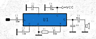
TA7066 amplifier circuit
Amplifier circuit is also very suitable when used in fm radio receiver. Supply voltage required 8 - 25 Volt DC with a maximum output power 0.15W.See Schematic below.
Part List
R1 = 100R
C1 = 1nF
C2 = 4.7uF
C3 = 10uF
C4 = 100uF
C5 = 47uF
C6 = 4.7nF
U1 = TA7066
Continue reading...

Sunday, April 7, 2013

Car Amplifier Care Tips

Car Amplifier Care Tips

car amplifier

Amplifier that work as one of the pillars of car audio does have ipandang performance that can not be underestimated. so we need to know a few things to keep our car amplifiers are not easily damaged. The following tips for creating a durable amplifier.


1. To install an amplifier on the audio systems in vehicles to avoid amplifier from moisture, the way while avoiding the base of potential placement into water vapor. so do not get into the inside of the amplifier resulting in damage to the components inside.

2. There is a good amplifier is used or not stored in a long time alias stored in a warehouse because after all the components within it requires a flow of current in accordance with nature as Conductor supply current to the driver other car audio.

3. Inside the vehicle, an amplifier should also be checked periodically, this is to find out the connection cable attached to the amplifier, amplifier kondiso also working actively to your car audio system.
Continue reading...

Saturday, April 6, 2013

Power Amplifier Protector

Now you can protect your HiFi amplifier from damage due to overheating. This circuit will cut off power to the amplifier board at the time the temperature was high. Automatically connect the power when the temperature returns to normal. This circuit uses a sensor NTC Thermister heat and also has a warning sound and reset determination.

Amplifier circuit protector is using popular timer IC NE 555 as the temperature controlled switch. The trigger pin 2 is connected to a potential divider consisting Thermister VR and NTC. Thus the voltage on pin 2 depending on the resilience and determination Thermister VR. NTC (Negative Temperature Coefficient) Thermister has a high resistance in the normal temperature and the resistance decreases as temperature increases. Threshold pin 6 of IC is used to reset the IC if necessary. When the pin 6 voltage gets higher than the IC pin 2 will reset and the output is low.

Power Amplifier Protector
Power Amplifier Protector  Circuits

Power to the amplifier board is given by (NC) contact is usually connected from the relay and the switch S2. So that power to the amplifier board will be available through the NC contacts of the relay when the relay S2 and the state is not powered. Thermister resistance is governed by VR triggering pin 2 of IC peaks at normal temperatures. When the temperature inside the cabinet amplifier increases, resistance decreases so that it becomes conductive Thermister. This makes the trigger pin 2 of IC is low and its output is high. T1 works so that the relay energizes and the ringing of a bell. This will damage the electrical supply to the amplifier board. Relay will not be automatically powered when the temperature returns to normal.

Amplifier circuit protectors are very useful to protect your home sound system.
Continue reading...

Friday, April 5, 2013

High Power Amplifier

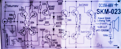
This circuit of power amplifiers using a booster 8 sets sanken , the buffer using transistor D400 and B560 as much 2 sets , and to use part of the driver transistor B546/A940 and D401/C2168. And least 20 volts and the voltage to 70 volts maximum with three voltage is +,-,ground. Power Output 2 X 600 Watt with 8 Ohm Impedance.
High Power Amplifier
Circuit audio amplifier 600 Watt

High Power Amplifier
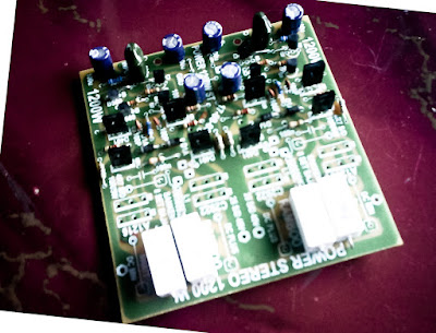
Circuit of PCB so from 2  X 600 watts (looked down)

Circuit of PCB (looked upon)

High Power Amplifier
The above is a circuit of ready to operate , just stay put booster.


Source : link
Continue reading...

Thursday, April 4, 2013

10W Audio Amplifier With Bass Boost


This design is based on the 18 Watt Audio Amplifier, and was developed mainly to satisfy the requests of correspondents unable to locate the TLE2141C chip. It uses the widespread NE5532 Dual IC but, obviously, its power output will be comprised in the 9.5 - 11.5W range, as the supply rails cannot exceed ±18V. As amplifiers of this kind are frequently used to drive small loudspeaker cabinets, the bass frequency range is rather sacrificed. Therefore a bass-boost control was inserted in the feedback loop of the amplifier, in order to overcome this problem without quality losses. The bass lift curve can reach a maximum of +16.4dB @ 50Hz. In any case, even when the bass control is rotated fully counterclockwise, the amplifier frequency response shows a gentle raising curve: +0.8dB @ 400Hz, +4.7dB @ 100Hz and +6dB @ 50Hz (referred to 1KHz).

Amplifier with Bass-Boost:
10W Bass Boost Amplifier Circuit DiagramParts:

P1_________________22K Log.Potentiometer (Dual-gang for stereo)
P2________________100K Log.Potentiometer (Dual-gang for stereo)
R1________________820R 1/4W Resistor
R2,R4,R8____________4K7 1/4W Resistors
R3________________500R 1/2W Trimmer Cermet
R5_________________82K 1/4W Resistor
R6,R7______________47K 1/4W Resistors
R9_________________10R 1/2W Resistor
R10__________________R22 4W Resistor (wirewound)
C1,C8_____________470nF 63V Polyester Capacitor
C2,C5_____________100µF 25V Electrolytic Capacitors
C3,C4_____________470µF 25V Electrolytic Capacitors
C6_________________47pF 63V Ceramic or Polystyrene Capacitor
C7_________________10nF 63V Polyester Capacitor
C9________________100nF 63V Polyester Capacitor
D1______________1N4148 75V 150mA Diode
IC1_____________NE5532 Low noise Dual Op-amp
Q1_______________BC547B 45V 100mA NPN Transistor
Q2_______________BC557B 45V 100mA PNP Transistor
Q3_______________TIP42A 60V 6A PNP Transistor
Q4_______________TIP41A 60V 6A NPN Transistor
J1__________________RCA audio input socket

Power Supply :
Power Supply Circuit DiagramPower supply parts:

R11_________________1K5 1/4W Resistor
C10,C11__________4700µF 25V Electrolytic Capacitors
D2________________100V 4A Diode bridge
D3________________5mm. Red LED
T1________________220V Primary, 12 + 12V Secondary 24-30VA Mains transformer
PL1_______________Male Mains plug
SW1_______________SPST Mains switch

Notes:
  • Can be directly connected to CD players, tuners and tape recorders.
  • Schematic shows left channel only, but C3, C4, IC1 and the power supply are common to both channels.
  • Numbers in parentheses show IC1 right channel pin connections.
  • A log type for P2 will ensure a more linear regulation of bass-boost.
  • Do not exceed 18 + 18V supply.
  • Q3 and Q4 must be mounted on heatsink.
  • D1 must be in thermal contact with Q1.
  • Quiescent current (best measured with an Avo-meter in series with Q3 Emitter) is not critical.
  • Set the volume control to the minimum and R3 to its minimum resistance.
  • Power-on the circuit and adjust R3 to read a current drawing of about 20 to 25mA.
  • Wait about 15 minutes, watch if the current is varying and readjust if necessary.
  • A correct grounding is very important to eliminate hum and ground loops. Connect to the same point the ground sides of J1, P1, C2, C3 &C4. Connect C9 to the output ground.
  • Then connect separately the input and output grounds to the power supply ground.
Technical data:
Output power:
10 Watt RMS into 8 Ohm (1KHz sinewave)
Sensitivity:
115 to 180mV input for 10W output (depending on P2 control position)
Frequency response:
See Comments above
Total harmonic distortion @ 1KHz:
0.1W 0.009% 1W 0.004% 10W 0.005%
Total harmonic distortion @ 100Hz:
0.1W 0.009% 1W 0.007% 10W 0.012%
Total harmonic distortion @ 10KHz:
0.1W 0.056% 1W 0.01% 10W 0.018%
Total harmonic distortion @ 100Hz and full boost:
1W 0.015% 10W 0.03%
Max. bass-boost referred to 1KHz:
400Hz = +5dB; 200Hz = +7.3dB; 100Hz = +12dB; 50Hz = +16.4dB; 30Hz = +13.3dB
Unconditionally stable on capacitive loads
Continue reading...

6 5W audio power amplifier

This amplifier circuit based on the ic, and the use here is that where ic STK4017 IC has output power of 6.5 watts with the impedance 8Ohm. Minimum required supply voltage and maximum 20Volt 35 Volt DC.
Component
R1 = 100K
R2 = 2K7
R3 = 27R
C1 = 22uF
C2 = 100uF
C3 = 100uF
C4 = 100uF
C5 = 100uF
C6 = 47uF
C7 = 330uF
C8 = 100uF
U1 = STK4017
Besides using STK4017 ic, ic and can use that I mentioned the following:
STK4019
STK4021
STK4023
STK4025
Continue reading...

Wednesday, April 3, 2013

Dayton Audio SA100 100W Subwoofer Amplifier

This Dayton Audio SA100 100 watt subwoofer amplifier with bendable crossover, climax and low level inputs, sports car on/rancid and part reverse switch is precise representing building your own powered subwoofer. Offers very calm undertaking with jam-packed overload protection.
Dayton Audio SA100 100W Subwoofer Amplifier
Technical Details
  • Low distortion audiophile sound
  • changeable low pass crossover
  • High and low level inputs/outputs
  • automobile On/rancid

Continue reading...

Tuesday, April 2, 2013

DC Coupled Audio Amplifier Circuit


This is a design circuit of audio amplifiers with DC coupling to the load are not often encountered these days, even though they offer definite advantages. One advantage is that there is no need for the complication of a second (symmetric) power supply; another is good frequency and phase response. Also, no special electrolytic capacitors are needed for voltage stabilization, and switch-on ‘thump’ is much reduced. This is the figure of the circuit;


It consists of a voltage divider, a voltage follower and the loudspeaker in the headphones, whose other side is connected to the junction of two electrolytic capacitors, providing the virtual earth. The potential at this point is, of course, half the supply voltage. All we need to do now is suitably couple in the audio signal to be amplified. This figure shows a practical realization of this idea in the form of a stereo headphone amplifier. The amplifier itself consists of IC1 and P1, R3 and R4 (giving a gain of 11). This part of the circuit demands no further explanation, and the same goes for the voltage divider mentioned above, formed by R1a and R1b. The signal is coupled in via the potentiometers. C2 and R2 have a special purpose: C2 connects the bottom end of the potentiometers (ground for the input signal) to the virtual earth. However, this capacitor creates a feedback path which can lead to oscillation of the amplifier under some circumstances. R2 damps this tendency to oscillate. It is possible to calculate suitable values for these components, but it is better to determine them by experiment. C2 must be sufficiently large that stray electric fields do not cause unacceptable hum at the output. R2 must be sufficiently large that the voltage at the amplifier’s virtual earth stabilizes quickly enough after switch-on. The polarity of the electrolytic is unimportant as no significant voltage appears across the network. It is possible to try the circuit out with the C2/R2 network shorted and observe the behavior of the circuit at switch-on using an oscilloscope. Depending on the degree of asymmetry in the circuit, the voltage at the virtual earth point can take a considerable time to stabilize.
Continue reading...

5000 Watts High Power Amplifier Schematic

Circuit Skema Rangkaian - High Power Amplifier has great advantages are 5000W ultra-light, high-power audio amplifier, without switching-mode power supply. This ambit is of an 2 x 2,500W RMS Stereo amplifier, super-light and after switching-mode ability supply. The ambit aloof shows a channel, and the ability accumulation that it assists to the two channels. The audio ambit should be duplicated, but the ability accumulation assists to the two channels after problems.
Circuit Skema Rangkaian Power Amplifier 5000W

A adapted affliction should be destined to the careful agent of the audio line, that should be of audio-high-quality, of the blazon acclimated in microphone pre amps ascribe line. The accomplished accumulation (2 channels) of 5,000W RMS it should not counterbalance added than 32 lbs, already central of an adapted brownish box.

WARNING:
This ambit is alone for abecedarian use. It contains not-isolated genitalia of the electric AC net and it can be actual dangerous. The access for the speakers are not abandoned of the calm AC net and it requests added care. This action seeks to acting a accepted ability accumulation with abundant weight and amount reduction, after necessarily to use a switching-mode ability supply.

This action cannot be accustomed in some countries for commercial-use. The columnist doesn’t accept any albatross for the anatomy as that ambit it will be applied.

> Related High Power Amplifier
>> 2800W High Power Amplifier Circuit
>>> 3000W Stereo Power Amplifier
>>>> 1500W HiFi Power Amplifier Circuit

Continue reading...