circuit harness wiring
Tuesday, February 4, 2014
Simple Voltage to Current Converter Drives White LEDs
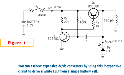
You sometimes need to drive a white LED from one 1.5V battery. Unfortunately, the forward voltage of a white LED is 3 to 4V. So, you would need a dc/dc converter to drive the LED from one battery. Using the simple circuit in Figure 1, you can drive one white LED or two series-connected green LEDs, using only a few components. The circuit is a voltage-to-current converter, which converts the battery voltage to a current that passes through the LED.
You can adjust this current and, thus, the brightness of the LED, by varying resistor R3. If you turn on switch S1, resistor R2 feeds base current to transistor Q2. Q2 turns on, and its collector current, via R3, turns on Q1. Now, the current through inductor L1 increases. The slope of the increase is a function of the value of L1 and the battery voltage. The current through L1 increases until it reaches a maximum value, which depends on the gain of Q1. Because the value of R3 sets the base current drawn from Q1, Q1s collector current is also limited.
White LEDs Circuit Diagram

Once the current through L1 reaches its maximum value, the slope of the current through L1 changes. At that instant, the voltage on L1 switches to a negative polarity forced by the changed slope. This negative voltage traverses capacitor C1 and turns off Q2, which in turn turns off Q1. The negative voltage on L1 increases until it reaches the forward voltage of the LED. The peak current through inductor L1 now flows through the LED and decreases to zero. Now, Q2 switches on again, via the current through R2, and the cycle starts again.
By adjusting resistor R3, you can set the peak current through L1 and the peak current through the LED. The brightness of an LED is a linear function of the current through the LED. So, adjusting the value of R3 also adjusts the brightness of the LED.
It doesnt matter which LED you use; the forward voltage on the LED always increases until the peak current through L1 flows through the LED. Different forward voltages of the LEDs yield different on-times (duty cycles) but the same peak current through the LED. With the values shown in Figure 1, the circuit oscillates at a frequency of approximately 30 kHz and delivers a 20-mA peak current through the LED.
The duty cycle depends on the ratio of the battery voltage to the forward voltage of the LED. One advantage of this circuit is that it requires no series-limiting resistor for the LED. The peak current through the LED is a function of the value of R3 and the gain of Q1.[via]
Continue reading...
You can adjust this current and, thus, the brightness of the LED, by varying resistor R3. If you turn on switch S1, resistor R2 feeds base current to transistor Q2. Q2 turns on, and its collector current, via R3, turns on Q1. Now, the current through inductor L1 increases. The slope of the increase is a function of the value of L1 and the battery voltage. The current through L1 increases until it reaches a maximum value, which depends on the gain of Q1. Because the value of R3 sets the base current drawn from Q1, Q1s collector current is also limited.
White LEDs Circuit Diagram

Once the current through L1 reaches its maximum value, the slope of the current through L1 changes. At that instant, the voltage on L1 switches to a negative polarity forced by the changed slope. This negative voltage traverses capacitor C1 and turns off Q2, which in turn turns off Q1. The negative voltage on L1 increases until it reaches the forward voltage of the LED. The peak current through inductor L1 now flows through the LED and decreases to zero. Now, Q2 switches on again, via the current through R2, and the cycle starts again.
By adjusting resistor R3, you can set the peak current through L1 and the peak current through the LED. The brightness of an LED is a linear function of the current through the LED. So, adjusting the value of R3 also adjusts the brightness of the LED.
It doesnt matter which LED you use; the forward voltage on the LED always increases until the peak current through L1 flows through the LED. Different forward voltages of the LEDs yield different on-times (duty cycles) but the same peak current through the LED. With the values shown in Figure 1, the circuit oscillates at a frequency of approximately 30 kHz and delivers a 20-mA peak current through the LED.
The duty cycle depends on the ratio of the battery voltage to the forward voltage of the LED. One advantage of this circuit is that it requires no series-limiting resistor for the LED. The peak current through the LED is a function of the value of R3 and the gain of Q1.[via]
Friday, January 10, 2014
Celsius Thermometer
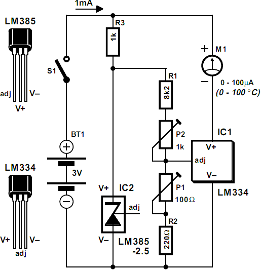
The circuit of the Celsius thermometer in the diagram is based on the well-known Type LM334 from National Semiconductor. This IC is a sensor that provides a current which is directly proportional to the temperature in kelvin (K). Unfortunately, this is a quantity that is not suitable for use in most practical applications. In the circuit, therefore, the sensor is set to 1µA K–1 with P1 and the offset of 273 K removed with P2.
This renders the output voltage of the sensor directly proportional to the temperature in degrees Celsius (° C) and this makes the circuit suitable for a great many applications (since 1K=1° C). Circuit IC2 is arranged as a 2.5 V reference voltage source. The current setting of the sensor is determined by the resistance between the adj(ust) pin and earth. If the earth is made virtual by raising the potential at the adj pin, the zero point can be shifted as desired. Calibration is best done by using a good domestic thermometer as reference.
Start by short-circuiting IC2 and adjusting P1 until the reading of meter M1 shows a current value numerically equal to the ambient temperature plus 273. If, say, the room temperature is 25°C, adjust P1 until the meter reads 298 µA. Then, remove the short-circuit from IC2 and adjust P2 until the meter reads a current whose numerical value is equal to the room temperature, that is, 25µA. The circuit draws a current not exceeding 1 mA, so using two AA size (AM3, MN1500, LR6, SP/HP7) batteries as power source will give a life of a couple of years.
Continue reading...
 |
| Celsius Thermometer Circuit Diagram |
This renders the output voltage of the sensor directly proportional to the temperature in degrees Celsius (° C) and this makes the circuit suitable for a great many applications (since 1K=1° C). Circuit IC2 is arranged as a 2.5 V reference voltage source. The current setting of the sensor is determined by the resistance between the adj(ust) pin and earth. If the earth is made virtual by raising the potential at the adj pin, the zero point can be shifted as desired. Calibration is best done by using a good domestic thermometer as reference.
Start by short-circuiting IC2 and adjusting P1 until the reading of meter M1 shows a current value numerically equal to the ambient temperature plus 273. If, say, the room temperature is 25°C, adjust P1 until the meter reads 298 µA. Then, remove the short-circuit from IC2 and adjust P2 until the meter reads a current whose numerical value is equal to the room temperature, that is, 25µA. The circuit draws a current not exceeding 1 mA, so using two AA size (AM3, MN1500, LR6, SP/HP7) batteries as power source will give a life of a couple of years.
Labels:
celsius,
thermometer
7MHz CW AM QRP TRANSMITTER
The circuit of a 7MHz C W / A M QRP transmitter described here can be used to transmit either CW or audio frequency Modulated signal over a 7MHz carrier.

The carrier frequency oscillator is crystal controlled using 7MHz crystal in its fundamental mode. The tank circuit comprises a shortwave oscillator coil which can be tuned to 7MHz frequency with the help of ½J gang capacitor VC1. Transistor T2 (with identical tank circuit connected at its collector as in case of transistor T1) serves as a power amplifier.
The RF output from oscillator stage is inductively coupled to the power amplifier stage. The output from power amplifier is routed via capacitor C3 and inductor L3 to a half-wave dipole using a 75-ohm coaxial cable. ½J gang capacitor VC3 along with inductor L3 forms an antenna tuning and matching network between the output of power amplifier stage and coaxial transmission line for maximum power transfer. Suitable heat sink should be used for transistor T2.
Tuning adjustments may be accomplished using a 6-volt torch bulb. Connect the bulb to the collector of transistor T1 first through a coupling capacitor and tune ½J gang VC1 for maximum brilliance. (Note: the bulb would light according to intensity of RF energy.) Same procedure may be repeated for power amplifier
stage and antenna tuning network for ensuring maximum power transfer. For CW operation, switch S1 is to be kept on for bypassing the audio driver transformer and Morse key is used for on/off-type modulation. CW would be generated during key depressions. For AF modulation, Morse key points should be closed and switch S1 should be flipped to ‘off ’ position. Any suitable mic. amplifier may be used to feed audio input to the audio driver transformer X1. (For transformer X1 you may use the transistor-radio type AF driver transformer.)
I would like to say that the transistor T1 is BF495. Power output of this circuit is about 150mW. It can be further increased by using separate power supply for the power-amplifier stage (24V, 1A). The coil details are as follows— L1 is short-wave oscillator coil; L2:14 turns on 1cm-diameter air-core tube using 26 SWG wire; L3 has 12 turns on 1.5cm-diameter air-core tube using 26 SWG wire.
The frequency allotted for amateur radio operators is 7.0 MHz to 7.1 MHz. Hence, any crystal available within this frequency can be used. Range of this QRP transmitter depends on propagation conditions. If conditions are good, the range is about 500 kms in the CW mode and 100 kms in the AM mode. It is possible to convert this transmitter to 20-meter HAM band. Any crystal available from 14 MHz to 14.350 MHz range can be used for the purpose. However, this conversion needs following modifications on coils L1, L2 and L3—L1: shortwave oscillator coil; L2: 11 turns on 1cm-diameter air-core tube using 26 SWG wire; L3: 9½ turns on 1cm-diameter aircore tube using 28 SWG wire.
An ammeter with a range 0-250mA or a multimeter with 0-250mA can be connected in-between the positive of the supply and the modulation transformer. Adjust VC1, VC2 and VC3 for maximum current through ammeter (CW-200mA, AM-125mA). The power input in CW and AM mode is calculated as shown below: DC power input (CW mode) = 24V x 250mA = 6watt (the power amplifier draws 250mA current). DC power input (AM mode) = 24V x 120mA = 2.8watt (the power amplifier draws 120mA current).
Labels:
7mhz,
am,
cw,
qrp,
transmitter
Thursday, January 9, 2014
100Khz Multiple Output Switching Power Supply Circuit Diagram
The 100Khz Multiple Output Switching Power Supply Circuit Diagram uses two VN4000A 400-V MOSPOWER FETs in a half-bridge power switch configuration. Outputs available are + 5 Vat 20 A and ±15 V (or ±12 V) at 1 A. Since linear three-terminal regulators are used for the low-current outputs, either ±12 V or ±15 V can be made available with a simple change in the transformer secondary windings.
A TU94 switching regulator IC proVides pulse-width modulation control and drive signals for the power supply. The upper MOSPOWER FET, Q7. in the power switch stage is driven by a simple transformer drive circuit. The lower MOS. Q6, since it is ground referenced. is directly driven from the control !C.
100Khz Multiple Output Switching Power Supply Circuit Diagram

The indication light on the host of cell phone jammer is red
The indication light on the host of cell phone jammer is red.
Operators network solutions business. Mobile infrastructure network devices, systems and solutions; microwave communication systems and solutions; optical networks solutions; IPTV solution; broadband solutions; mobile communications applications and value-added service solutions for design, development, systems integration and sales; communication software development, design and system integration, and the system equipment, the end product engineering, maintenance and consulting business. History of the development of the mobile phone industry. China mobile phone the course of development can be divided into the era of analog phones, the GSM era era and the era of 3G, 2.5G, 3G represents the development trend of Chinas mobile phone. If the customer wants to disguise the use of cell phone jammer .
The era of analog phones, probably from China Mobile Communications Corporation began operations in 1987 900MHz analog mobile phone service date to December 31, 2001, China Mobile Communications Corporation is the complete cessation of analog mobile phone network customers international and domestic roaming services cut-off. After this, the mobile phone by the analog to digital development, including the rapid development of GSM and CDMA digital mobile phone standard worldwide. In the 1980s, the global mobile phone business is growing very fast. The late 1980s, the global use of wireless telephone terminal users, the number of annual growth rate of 40 percent, far more than the same period the annual growth rate of fixed line telephone users.
Macro environmental factors of the mobile phone industry. Political - legal factors. Specifically, some government action restrictive role in the activities of the enterprises, but some government policy guidance and a positive impact on the enterprise. In accordance with Chinas WTO accession commitments, December 11, 2004, China canceled the limitations of geography, equity and the number of foreign-invested commercial enterprises in Chinas retail sector is opened to all. So that the domestic retail market capacity is rapidly expanding, industry, competition is fiercer than ever. Generally speaking, in the case of macroeconomic development, market expansion and increased demand for business development opportunities. Beginning in 2003, Chinas central governments macro-control targets are mainly concentrated in four areas. It is the high performance heat dissipation chip of cell phone jammer .
Gross domestic product (GDP) growth in the number of degrees, the general price level, the urban unemployment rate or the level of employment, the international balance of payments status.
Continue reading...
Operators network solutions business. Mobile infrastructure network devices, systems and solutions; microwave communication systems and solutions; optical networks solutions; IPTV solution; broadband solutions; mobile communications applications and value-added service solutions for design, development, systems integration and sales; communication software development, design and system integration, and the system equipment, the end product engineering, maintenance and consulting business. History of the development of the mobile phone industry. China mobile phone the course of development can be divided into the era of analog phones, the GSM era era and the era of 3G, 2.5G, 3G represents the development trend of Chinas mobile phone. If the customer wants to disguise the use of cell phone jammer .
The era of analog phones, probably from China Mobile Communications Corporation began operations in 1987 900MHz analog mobile phone service date to December 31, 2001, China Mobile Communications Corporation is the complete cessation of analog mobile phone network customers international and domestic roaming services cut-off. After this, the mobile phone by the analog to digital development, including the rapid development of GSM and CDMA digital mobile phone standard worldwide. In the 1980s, the global mobile phone business is growing very fast. The late 1980s, the global use of wireless telephone terminal users, the number of annual growth rate of 40 percent, far more than the same period the annual growth rate of fixed line telephone users.
Macro environmental factors of the mobile phone industry. Political - legal factors. Specifically, some government action restrictive role in the activities of the enterprises, but some government policy guidance and a positive impact on the enterprise. In accordance with Chinas WTO accession commitments, December 11, 2004, China canceled the limitations of geography, equity and the number of foreign-invested commercial enterprises in Chinas retail sector is opened to all. So that the domestic retail market capacity is rapidly expanding, industry, competition is fiercer than ever. Generally speaking, in the case of macroeconomic development, market expansion and increased demand for business development opportunities. Beginning in 2003, Chinas central governments macro-control targets are mainly concentrated in four areas. It is the high performance heat dissipation chip of cell phone jammer .
Gross domestic product (GDP) growth in the number of degrees, the general price level, the urban unemployment rate or the level of employment, the international balance of payments status.
Subscribe to:
Comments (Atom)