Tuesday, April 30, 2013

Simple Solar charger circuit project using transistors

A very simple solar charger circuit project can be designed using few external electronic parts . This simple solar charger circuit is capable of handling charge currents of up to 1A. Alternate component values are given in the figure for lower current applications.

Circuit diagram:
12V-SLA-chargher Solar charger circuit project using transistors circuit diagram

The only adjustment is the voltage trip point when the current is shunted through the transistor and load resistor. This should be set with a fully charged battery. As the transistor and R3 have the entire panel’s output across them when the battery is fully charged, all of the current from the panel will be going through R3 and the Darlington transistor TIP112, so these must be well heat sunk. Adjust R1 for the trip point, usually 14.4 V – 15 V for a 12 V SLA or a 12 V Ni-Cd battery.

Continue reading...

Sunday, April 21, 2013

DUAL 3v WHITE LED FLASHER DUAL 1v5 WHITE LED FLASHER


This circuit alternately flashes 2 white LEDs, on a 3v supply and produces a really bright flash. The circuit produces a voltage above 5v if the LED isnt in circuit however the LED limits the voltage to its characteristic
voltage of three.2v to 3.6v.   The circuit takes concerning 2mA and is actually a voltage-doubler (voltage incrementer) arrangement.

The 1k charges the 100u and therefore the diode drops zero.6v to prevent the LED from setting out to illuminate on 3v. When a transistor conducts, the collector pulls the 100u down towards the 0v rail and therefore the negative of the electro is actually concerning 2v below the 0v rail. The LED sees 3v + 2v and illuminates terribly brightly when the voltage reaches about 3.4v.  All the energy within the electro is pumped into the LED to supply a really bright flash.

DUAL 1v5 WHITE LED FLASHER

This circuit alternately flashes 2 white LEDs, on a 1.5v supply and produces a really bright flash. The circuit
produces a voltage of concerning 25v when the LEDs dont seem to be connected, however the LEDs scale back this as they need a characteristic voltage-drop across them after they are illuminated. dont use a offer voltage above one.5v.

The circuit takes concerning 10mA. The transformer consists of thirty turns of terribly fine wire on a 1.6mm slug 6mm long, however any ferrite bead or slug will be used. the amount of turns isnt crucial. The 1n is very important and using the other worth or connecting it to the positive line can increase the provision current.
Using LEDs apart from white can alter the flash-rate considerably and each LEDs should be identical color.

Continue reading...

Saturday, April 13, 2013

Tuned Radio Frequency TRF Receiver

Super heterodyne receivers have been heavily produced due to the fact round 1924, but for reasons of value did not become a hit except the Nineteen Thirties. Before the 2d world war different, more practical receiver technologies any suchs the TRF receiver and the regenerative receiver were nonetheless popular.

Circuit diagram :
 
Tuned Radio Frequency (TRF) Receiver Circuit Diagram

The circuit described here is in accordance with the old technology, however brought updated a The most vital part of the circuit is the input stage, the place certain comments is used to reach good sensitivity and selectivity. The first stage is adjusted in order that it isn't moderately on the level of oscillation. This will increase the gain and the selectivity, giving a slender bandwidth. To do so, the potentiometer connected to the drain of the FET need to be adjusted very carefully: top-quality efficiency of the receiver depends on its environment. In best prerequisites a couple of strong stations must be out there right through the day the use of a 50 cm antenna. At night time, several times this number should be available.

The frequency range of the receiver runs from 6 MHz to 8 MHz. This vary quilts the forty nine m and the forty one m shortwave bands during which many European stations broad-cast. Not bad for one of these easy circuit! The circuit appoints six transistors. The first stage is a selective amplifier, followed via a transistor detector. Two low-frequency amplifier degrees full the circuit. The last stage is a push-pull arrangement for most effective force of the low-impedance loud-speaker. This circuit association is some-times referred to as a ‘1V2 receiver’ (one preamplifier, one detector and two audio frequency ranges).

Setting-up is easy. Adjust P1 unless the purpose is reached the place the circuit starts to oscillate: a whistle might be heard from the loudspeaker. Now back off the potentiometer except the whistle stops. The receiver can now be tuned to a broad-caster. Occasional further adjustment of the potentiometer is also required after the station is tuned in.  The receiver functions from a provide volt-age of between 5 V and 12 V and makes use of little or no current. A 9 V PP3 (6F22) battery will have to give an extraordinarily long life.


 http://www.ecircuitslab.com/2012/02/tuned-radio-frequency-trf-receiver.html
Continue reading...

Junk box Fan Speed Controller

My new house theatre receiver used to be getting relatively scorching in the shut confines of its cabinet, with the temperature attaining over 40°C after handiest about half-hour of use. To lend a hand lower the temperature, I decided to install a fan within the cabinet. A 75mm hole used to be lower in the shelf beneath the receiver, and a 12V fan salvaged from an outdated computer energy provide was installed beneath. The fan used to be powered from a 12V DC plugpack. 

This did the job, maintaining the temperature under 30°C even after prolonged use on a heat day. However, the fan was once annoyingly loud when operating at full speed. To reduce the noise degree notably, I constructed this fan pace controller with temperature comments. The circuit was culled from number of concepts found on various websites on the web, with the final circuit designed from what was once within the \"junk box\". Air temperature in the cabinet is sensed via an LM335 (TS1).

Circuit diagram:
Junk-box Fan Speed Controller Circuit Diagram

It is glued to a section of aluminium about 25mm square with fast glue, which is then connected to the highest of the receiver with \"Blue-Tack\". About 300mm of audio coax makes the connection back to the circuit board. The LM335’s output upward pushs 10mV per diploma Centigrade. It is calibrated to zero output at -273°C, so at 20°C, the output will doubtless be 2.93V. This is applied to the non-inverting input of a 741 op amp (IC1). A 1N4733 5.1V Zener diode gives a voltage reference for the inverting input via trimpot VR1. The output of the op amp forces a TIP122 Darlington transistor (Q1), which in flip pressures the fan motor. The op amp gain was once calculated to provide about 12V to the fan at 40°C. 
 
To keep the transistor cool, it's set up on the metal base of a small plastic field, which is also used to accommodate the elements.  Initial setup will have to be carried out with everything turned off and the ambient temperature at about 20°C. Adjust the 10-turn pot except the fan just stops running. I used a gasket comprised of foam strips and \"blue-tacked\" them between the feet of the receiver to direct all the airflow by way of it. The temperature now remains at about 32°C, the fan runs very quietly and continues to run down for approximately 30 minutes after the receiver is switched off.


Author: Martin Cook - Copyright: Silicon Chip Electronics
Continue reading...

5 Zone Alarm System

This is an entire alarm system with 5 impartial zones appropriate for a small place of business or home environment. It uses just 3 CMOS ICs and includes a timed entry / exit zone, 4 fast zones and a panic howeverton. There are indicators for each zone a \"system armed\" indicator. The schematic is as practices:


\"5


Circuit Notes
Each zone makes use of a generally closed contact. These can be micro changees or usual alarm contacts (usually reed switches). Suitable switches can also be bought from alarm shops and hid in door bodys, or window ledges.

Zone 1 is a timed zone which need to be used because the entry and exit point of the constructing. Zones 2 - 5 are fast zones, for you to trigger the alarm with out a delay. Some RF immunity is presentd for lengthy wiring runs by the input capacitors, C1-C5. C7 and R14 also kind a transient suppressor. The key change acts as the Set/Unset and Reset change. For just right security this must be the metallic kind with a key.

Operation
At change on, C6 will cost by approach of R11, this acts because the exit extend and that is set to round 30 2nds. This may also be altered through varying either C6 or R11. Once the timing length has elapsed, LED6 will mild, which implys the device is armed. LED6 could additionally be installed externally (at the bell box for example) and provides visual indication that the device has set. Once set any contact that opens will set off the alarm, including Zone 1. To stop set offing the alarm on entry to the constructing, the concealed re-entry change need to be functiond. This will discharge C6 and begin the entry timer. The re-entry change can be a hid reed swap, positioned anywhere in a door frame, however invisible to the attention. The panic swap, when pressed, will trigger the alarm when set. Relay contacts RLA1 provide the latch, RLA2 operate the siren or buzzer.


Author : Andy Collinson
Continue reading...

Friday, April 12, 2013

4 X 15 Watt Mini Power Amplifier

A lot of electronic circuits in the domain of audio amplifiers are already been published here. This circuit is a little different because it is a four channel amplifier. Each channel of this amplifier can deliver an output of 15Watts into a 4 ohm speaker. The amplifier can be operated from a single 12V DC supply and this makes it possible to use this amplifier in car audio applications too.

Circuit diagram :
4X15W-amplifier-circuit Diagram
4 X 15 Watt Mini Power Amplifier

The circuit is based on the 15W BTL X 2 channel audio power amplifier IC TA8215 from Toshiba. Even though chip is specifically designed for car audio applications it can be also used for home audio applications. Two TA8215 ICs are used here in order to obtain a 4 channel amplifier system. The circuit is designed almost exactly as per the application diagram in the ICs datasheet. Pins 7 and 19 are the Vcc pins of the ICs internal integrated power amplifier stages and these pins are connected to the positive supply. Pin 9 is the Vcc pin for ICs internal preamplifier and it is also connected to the positive supply. Pins 13 and 14 are the internal power amplifiers ground pins and they are tied together and connected to the ground. 

The internal preamplifier’s ground pin (pin5) is connected to the common ground through a 10 Ohm resistor which makes the input ground separated from the common ground by a resistance of 10 ohms and this improves the noise rejection. The 100uF capacitor works as a power supply de-coupler. The resistor networks connected to the output lines of each amplifier improves the high frequency stability. The variable resistors (R3, R4, R12 and R13) works as the volume controller for the corresponding channels.

Notes :
  • Assembling the circuit on a good quality PCB is a must for obtaining optimum sound quality.
  • Use 12V DC for powering the circuit.
  • The ICs must be fitted with adequately sized heat sinks.
  • R3, R4, R12 and R13 serves as volume controllers.
  • K1 to K4 can be 4 Ohm, 20W speakers.
  • This amplifier circuit can be used in a variety of applications such as car audio systems, home theater systems, personal audio systems, public address systems etc. link
Continue reading...

Smoke detector circuit

This causes the resistance of LDR to increase and the voltage at the base of the transistor is pulled high due to which the supply to the COB (chip-on-board) is completed. The sensitivity of the smoke detector depends on the distance between bulb and LDR as well as setting of preset VR1.
Thus by placing the bulb and the LDR at appropriate distances, one may vary preset VR1 to get optimum sensitivity.
We have not build this smoke alarm detector.

For smoke detector installation and maintenance use a near electrician.
Continue reading...

Hydrophone Booster Amplifier HA2

Hydrophone Booster Amplifier (HA2)
The HP series Hydrophone Booster Amplifier (HA2) amplifies low-level hydrophone signals over a wide range of frequencies. It has a minimum gain of 25dB and an input and output impedance of 50Ω. The HA2 is designed for use with either Precision Acoustics membrane hydrophone or Precision Acoustics HP Series Hydrophone Measurement System, which is shown in Fig 1.
Hydrophone Booster Amplifier
Alternatively, the HA2 may be used when the acoustic signal is provided by a high output impedance hydrophone, such as a GEC-Marconi membrane device, or a conventional hydrophone. In this instance a BNC/MCX adaptor is used which connects directly to the HP Series Submersible Preamplifier, using it as a buffer amplifier, (i.e. the standard Precision Acoustic HP Series configuration shown in Fig 1 is used, but without the interchangeable probe).
The HA2 amplifier is straightforward to use but the following points should be noted:
  • The output of the amplifier should be correctly terminated in 50Ω before operation.
  • The HA2 amplifier is non-inverting but this is of no consequence when used with the HP Series interchangeable probes as their design takes this into account. However when a submersible preamplifier is used as a high impedance buffer amplifier (as in Fig 2) the system output from the HA2 will be inverted as the HP Series Submersible Preamplifier is inverting.
Before Connecting the unit please read WARNING
To Connect
To  Disconnect
1 Connect Output Load 1 Remove RF Input
2 Apply DC Voltage 2 Remove DC Volts
3 Apply RF Input 3 Remove Load

Specification (HA2 Amplifier Only)
Voltage Gain = 25dB minimum
Bandwidth =  50kHz to 125MHz ±1.0dB
Maximum Output Level = 29dBm for 1dB compression (18.1V pk – pk into 50Ω load)
Input Impedance = Nominal 50Ω
Output Impedance  Nominal 50Ω (VSWR 2:1)
Output Noise Level = Typically 70μV pk – pk (bandwidth 125MHz)
Noise Figure = Typically 10dB
Phase = Non-inverting
Terminations:
Front panel = Input BNC socket BNC Output socket
Rear panel Power Requirements = 28v dc output to supply DC Coupler 100/120/220/240V ac, 50 to 60Hz,
7.5W
Operating Temperature = 0 to 50°C
Size = (90mm × 205mm ×194mm)
Weight = 2.6kg


Streampowers
Continue reading...

Garage Stop Light

A novel use of solar cells makes positioning your car in the garage rather easier than old tyres, a mirror, or a chalk mark. The six solar cells in figure 1 serve as power supply and as proximity sensor. They are commercially available at relative low cost. The voltage developed across potentiometer Pi is mainly dependent on the intensity of the light falling onto the cells. The circuit is only actuated when the main beam of one of the cars headlights shines direct onto the cells from a distance of about 200 mm (8 inches). The distance can be varied somewhat with P,

Simple Garage Stop Light Circuit Diagram :

Simple-Garage-Stop-Light-Circuit Diagram

Under those conditions, the voltage developed across C1 is about 3 V, which is sufficient to trigger relaxation oscillator Ni. The BC547B is then switched on via buffer N2 so that D3 begins to  lfash. Diodes Di and D2 provide an additional in- crease in the threshold of the circuit. The total voltage drop of 1.2 V across them ensures that the  potential at pin I of the 4093 is always 1.2 V below the voltage developed by the solar cells. As the trip  level of Ni lies at about 50 per cent of the supply  voltage, the oscillator will only start when the supply voltage is higher than 2.4 V.

The circuit, including the solar cells, is best constructed on a small veroboard as shown in figure 3, and then fitted in a translucent or transparent man- made fibre case. The case is fitted onto the garage wall in a position where one of the cars headlights shines direct onto it. The LED is fitted onto the same wall, but a little higher so that it is in easy view of the driver of the car. When you drive into the garage, you must, of course, remember to switch on the main beam of your headlights!

Source : www.ecircuitslab.com
Continue reading...

Video IF circuit TV

Video IF circuit
Video IF circuit
The main function of the video IF is to change the 38.0 MHz IF signal into the CVBS signal which later fed into the sound and video to the chroma.


VIF section consists of a series as follows:
IF amplifier
This section serves to strengthen the signal until the signal level is required. IF amplifier is equipped with AGC (Automatic Gain Controller) which controls the strengthening of the IF amplifier so that a constant amplitude output video. Amplifier frequency range from 32 ~ 60 MHz makes this amplifier suitable for applications multistandar.

PLL demodulator and VCO (voltage control oscillator)
IF signal is separated with the help of PLL detector. PLL detector produces a phase reference signal with the IF signal carrier and about 60 KHz bandwidth is determined by PLL loopfilter pin 37. Obtained by comparing the frequency demodulation reference signal with the incoming IF signal. Are required reference frequency (38.0 MHz) generated by the VCO. Appropriate VCO frequency is determined by system calibration using the crystal as a reference. PLL can detect the IF frequency up to ± 1 MHz based on FPLL (Frequency Phase Lock Loop System) which will provide an output signal to the PLL loopfilter for the difference frequency is obtained. If the phase IF signal with a reference signal, the signal is transmitted to the demodulator. Demodulator to control the positive and negative modulation, the selection made ​​by the IIC bus. Low pass filter after the output signal demodulator eliminates the demodulation is not required to process the video.

Video IF schematics


Video Buffer
Video buffer to produce a video output with an amplitude of the right and keep the video output from the noise peak occurring. The bandwidth of the video buffer at least 6 MHz. In the video there are White spot clamp buffer (for positive modulation) and the noise inverter Clamp (for negative modulation) which keeps the amplitude of the video does not exceed the typical price.

Continue reading...

Measuring Milliohms with a Multimeter

Low values of resistance can be troublesome especially when large current s f low through them. A current of, say, 10 A passing through a terminal with a contact resistance of 50 m? will produce a voltage difference of 0.5 V. This resulting power loss of five watts is dissipated in the termination and can give rise to a dangerously high temperature which may degrade insulation around the wires.

Measuring Milliohms with a Multimeter Circuit Diagram

Measuring Milliohms with a Multimeter-Circuit Diagram

Measuring low values of resistance is not easy. Low cost multimeters do not include a milliohm measurement range and specialist equipment is expensive. The simple circuit described here allows milliohm measurements to be made safely on a standard ist equipment is expensive. The simple circuit described here allows milliohm measurements to be made safely on a standard multimeter. The circuit consists of little more than a 6 V voltage regulator and a mains adapter capable of supplying around 300 mA at 9 to 12 V.

The circuit supplies a fixed cur-rent output of 100 mA or 10 mA selected by switch S1. This connects either the 60 ? or 600 ? resistor into the constant current generator circuit. The resistor values are produced by paralleling two identical resistors; 120 ? and 1.2 k? from the E12 standard resistor range. Two test leads with probes are used to deliver current to the test resistance. The resultant voltage drop is measured by the multimeter (M1). With the test current set to100 mA a measurement of 1 mV indicates a resistance of 10 m?. At 10 mA (with S1 in the position shown in the diagram) a measurement of 1 mV indicates a resistance of 100 m? while 0.1 mV is equal to 1 m?. Diode D1 protects the meter from too high an input voltage.

With the voltmeter connected as shown in the diagram it measures not only the voltage drop across RX but also that produced by the resistance of the test leads, and probes. To make a true measurement, first touch the probes close together on the same lead of the test resistance and note the reading, now place the probes across the test resistance and note the reading again. The first reading measures just the test leads and probes while the second includes the resistance RX. Subtract the first measurement from the second to get the value of RX.

The accuracy of the measurements are influenced by the contact resistance of switch S1, the precision of resistors R1 to R4, the 6 V supply level and of course the accuracy of the measuring voltmeter. For optimum decoupling C1 should be fitted as close as possible to pin1 of IC1. An additional electrolytic capacitor of around 500 µF can be used at the input to the circuit if the input voltage from the AC power adapter exhibits excessive ripple.

Source:  http://www.ecircuitslab.com/2012/03/measuring-milliohms-with-multimeter.html
Continue reading...

Phone Recorder Circuit

This is a schematic for recording the conversation in telephone. One constructed, this switch will allows you to automatically turn on your tape recorder when you pick up the handset of your telephone. This circuit is designed to work for the newer 1.5V and 3V tape recorders as well as the usual 6V or 12V ones. This circuit is control based on transistor and FET’s. Looking in the figure of schematic.


The circuit is fall into two part and these can be easily seen in the schematic. On the left are the connections to each telephone line and to the MIC socket of the tape recorder. The diode and capacitors ensure that no DC voltages pass through to the input of the MIC while the RC network clips large transients. On the right is the circuit which detects when the handset has been lifted and which then turns on the FET. The trim pot adjusts the voltage level of this circuit. The voltage of the normal telephone line is between 40 to 60 volts (depending on country and telephone system.) When you pick up the handset of the telephone the voltage falls to between 6 and 12 volts. It is this drop in voltage which is used to control the tape recorder through the REMOTE connector. When the line voltage is high the base of the BC548 is pulled high so the transistor is turned on. This pulls the gate of the FET down to less than 1 volt. This shuts off the FET.

When the line voltage falls (that is, the handset is picked up) the BC548 will turn off, adjust the variable resistor if it does not. So the FET gate potential rises to the 10 volts set by the zener diode. This turns the FET on to high efficiency conduction mode. Different recorders may have different polarities in their REMOTE sockets. To allow for this a PCB mounted switch has to be added to the board which will reverse the polarity of the REMOTE switch just by switching it.


Continue reading...

Thursday, April 11, 2013

Transceiver Homebrew QRP SSB 80M Band

Radio communication transceiver is a radio transmitter at the same time the plane doubles as a radio receiver used for communication purposes.
It consists of the transmitter and the receiver are assembled in an integrated way. In mulamula generation, the transmitter or receiver or transmitter and receiver sections are assembled separately and is part of a stand sendirisendiri and can work well sendirisendiri Currently employed both parts are integrated in turn.


Transceiver Homebrew QRP SSB 80M Band


Aircraft simple transmitter consists of an oscillator generating radio vibration and this vibration after vibration boarded with our voice, in a technique called dimodulir radio, then by the antenna is converted into radio waves and transmitted. As we know that the sound waves we can not reach long distances, although its power is quite large, while the radio waves with a relatively small force can reach a distance of thousands of kilometers. In order for our voice can reach a far distance, then our voice superimposed on radio wave radio results from the vibration generator, called a carrier wave or carrier and the carrier wave was going to deliver our voice to distant places.


In a place far earlier, the radio waves emitted by the antenna received our speaker. By the antenna, radio waves had, in the form of electromagnetic waves is converted into electrical vibrations and into the receiver.


In our speaker receiver plane, vibration and vibration carriernya then discarded and then raised our voices be accommodated through the speakers. With this technique it is possible modilasi an audio vibrations reach a far range.


We sound vibrations enter the transmitter through a microphone, microphone output was often needs to be strengthened first with an audio amplifier is called a microphone preamplifier can be superimposed on the carrier for the modulator.


To increase the transmission power of a transmitter, vibration of the oscillator was before the emitted amplified first with a radio frequncy amplifier. Strengthening can be done once and can also be done more than once. Transmitter is not reinforced is called a level transmitter and the reinforced one called two-level and beyond. In general, to reach 100 Watt transmit power need to strengthen the 3 times, the first amplifier is called predriver, the next amplifier called the driver and final amplifier called the final amplifier.


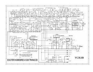
Block Diagram of SSB Transceiver


If were talking about the Single Side Band, then we touched more on amplitude modulation (AM). At each modulation we do we actually do the mixing between the radio frequency to audio frequency. Any mixing of two frequencies will occur the second summation process and at the same frequency reduction process occurs from both frequencies.


So every time we memodulir carrier, will produce two frequencies at once. For example, a carrier with a frequency of 3000 Kc we modulir with audio ferkuensi 3 Kc, the result is 3003 Kc and Kc 2997, or said occurred two sides of the band is the upper side and lower side. The top side and bottom side are shaped symetris, so if it is a direct result of modulation we mean we memancarakan exude the same two goods.


If we shine the way mentioned above, we use the mode is said to Double Side Band (DSB) because the carrier that includes top and bottom sides are emitted together. In factory-made plane, this mode is usually coded in terms actual AM radio is the DSB technique.


We know there are two kinds of ways to make the SSB, the first way is by phase shift method, another way is by filtering methods. The first way is not widely used and factory-made aircraft SSB generally use filtering.


Signal DSBSC, before the amplified and transmitted, is inserted into the SSB filter in advance to produce LSB or USB. Filters are used for this purpose is filtering crystal or mechanical filters. SSB transmitter is said to be more efficient than AM (DSB), we can give this picture as follows. For example transmitter AM (DSB) with power 150 Watt (100% modulation depth), then power on the USB and LSB respectively and the carrier has a 25 Watt 100 Watt power. We know that the audio side we are on the band. In the SSB emission, emitted only one side band LSB or USB is a powernya only 25 Watt.


With SSB 25 Watt beam, the audio we have to arrive at destination with the same clarity of information with jet AM (DSB) 150 Watt earlier.


Another advantage of SSB is the wide-band mode that can be more narrow. For the purposes of communication, SSB mode requires only the band width of about 3 Kc, while the DSB mode takes about 6 Kc, thus providing savings SSB mode the use of the band.


In the detector a SSB receiver, the received signal must be mixed in advance with the frequency of the outcome of a Beat Frequency Oscillator (BFO) and used as the BFO carrier oscillator.


Homebrew QRP SSB Transceiver circuit 80m Band


In general, the transceiver has the following block diagram, basically Transceiver tebagi into three main parts: Part VFO and BFO Part Transmitter (transmitter) and Section Receiver (receiver), where there are some special blocks that are used for both paths are either transmitter or receiver. Simply in this transceiver merkit Use the tools that we only Multi tester, RF Probe, SWR and Power Meter, Tone Generator Af 1Kc and multi-band Radio HF SSB to function as a monitor frequency BFO, VFO, monitor Balanced Modulator Exciter at once both the transmitter or receivers .


Data Transceiver:


Frekwency Range: 3700 Kc a / d 3900 Kc


Mode: LSB Singgle conversi


IF: 455 Kc (Ceramic Filter SFU type 455)


Local oscillator: VFO with Fine Tuning varactor diode


BFO: Ceramic Filter 455 SFU


RF PA: Power FET IRF640, IRF540, IRFZ44


DC: 13.8 V


RF Power: Over 8Watt


Description Schema.


The order of assembly sequence of assembling consecutive start BFO, VFO, AF Amp, IF amplifier and detector products to filter amplifier circuit, Mic Amplifier, Balanced modulator, RX mixer + Rf amplifier, mixer TX last order to facilitate the checking of each unit due to series This is a merger of several units of its own circuit.


BFO.


Memprgunakan SFU type ceramic filters used 455 two-foot middle leg to ground is coupled with capacitor and capacitor trimer and one leg edges to the base of the transistor, BFO uses two types of 2SC1815 transistors. Tc 1 to set the BFO on 453.5Kc frekwensy being black 455Kc IF transformer to regulate the level rather than BFO. To check this The set uses RF Probe. At the secondary BFO output T9 check with RF probe set T9 smpai maximum output level monitor in the radio frequency or HF trimer and Counter set Capacitor capacitor pararelnya until fulfilled the required frequency of 453.5Kc. To check whether there are oscillations in the BFO off Ceramik filter whether RF probe was still moving when he checks it again rangakain ceramik here if we filter out the RF probe is not moving.


VFO.


For we use the VFO FET 2SK192 Type and reinforced with a single fruit type transistor 2SC1815. Raft of this series as neat munkin with component selection, especially capacitor here we use a paper capacitor in series of Colpits oscillator. Close this series with a metal box along with all Varconya. VFO same testing with the BFO circuit Trime Koker Ferrite T13 dapakan frequency monitor the frequency of 4100 Kc s / d 4300 Kc obtained in case of no frequency range is set set the number of coil and capacitor values ​​bypas to groundnya.


AF amplifier.


AF Amplifier IC type LM386 used raft this section and check out by Spiker at putnya. Plug the foot of its inputs with a screwdriver had no defects at the time vulume potensio enlarged.


IF AMP AND PRODUCT detector.


Raft had Produc detectornya from starting until the fourth diode 1N60 IF transformer T7 455 black color until the transformer bypass capacitor to ground. Plug one side of the transformer with a screwdriver kai harden the audio volume on the speakers should be no reaction. Attach the amplifier transistor for testing at its base on the speaker should be louder voice. Raft this section everything.


FILTER amplifier.


Put all the components properly to eighth ceramic filter installed all. Just listen to the speaker plug on the input or pairs if a small number of meters of cable serves as an antenna trim T6 and T8 listen to the voice on the speaker until no defects dispeaker be hissed loudly.


RX MIXER AND RF amplifiers.


This series of rafts with the good and right in making the winding must be in a state of neat. Enter Snyal VFO to try to monitor the input mixer is QSO friends turn ferrite in successive Koker turu of T3 and T4 to get a strong signal reception and set the T1 and T2 ferrite to signal strong receipts received with respect to the level of the S Meter. If that is not found try to check this section further. Thus selesei weve Section Receiver unit.


MIC amplifier.


Raft of this section and replace all the LM 741 IC listen with headphones turn out putnya potensio putnya try out the level of talk in the microphone must be perfect without any defects in the out putnya.


BALANCE modulator.

Balanced modulator uses AN612 ic type commonly used on the CB radio. Raft all components correctly. To check this series of pairs of probes to the output at ic AN612 when no signal on the IC probe set trimpot until the deviation of zero and then try to plug in with tweezers pda mic input amplifier should have needle probe deviation. Then plug micropon try talking meter on the probe to move the motion according to your speech input level. Put some small cable length as the antenna you are trying to monitor diradio HF signal here was DSB Uper and Lower Side band sound. Dengarka until there is no defect here is selesei sets. Then go Filter amplifier output to try to talk Rangkian denagan put up some yards kabbel to secondary T6 try IF 455 White color monitor frequency of 455 Kc diradio on and try to talk trim ferrite Ferrite T6 and T8 until you hear the sound on USB diradio no oscillation and no deviation selef the meter on the probe. If on your radio monitors have didapatka perfect sound means youve selesei at once to part If rceifernya.


TX MIXER.

Raft section make this all too well circumference at T11 and T12 as neat as possible. Mixer that we use the type of premises IC TA7310 2SC1815 transistor amplifier pairs as well. Then plug VFO output and Out put Balnce Modulatornya on laulu TA7310 ic input probe pairs give the mic input with tone generator af ferrite trim T11 and T12 refer to deviation meter probe to obtain the largest deviation meter. Put microppon try talking dimicropon deviation meter see if were not talking micropon but no deviation on the meter needle probe set trim T11 and T12 until no deviation in meters try to talk again in micropon deviation meter should move according to their level talks on the microphone. Try installing a few meters of the small wires on the monitor amplifier output tx diradio exciter in accordance with the frequency of our work with the fashion side band LSB if we do not get on the LSB mode with sempurana set again trimer capacitor on the BFO and rotate slightly if T8 transformer ferrite in black color smpai obtained side band we want. Up here seleseilah exciter circuit.


TX PA amplifier.

PA series we take the type of Power FET because it is cheap and easily available in the market. Create a transformer with a good and right not to email pda scuffed pair of wires until there is a first level transistor 2SC1815 output pairs of probes on trying to talk on the microphone deviation at Beh probe must be greater than the level of exciter here should not happen if not self-oscillation oscillation talk there is no deviation on the meter needle probe. In the event of self-oscillation try to check the part. Similarly, the driver assembly. Drivers are taking transistor type 2 SC1162. gained power level meter must be greater than the previous level as well. Then the final units also make coils as neat as possible. Testing out first input of the exciter arur Pa measuring voltage trimpot should not exceed 3V plug out put a probe hyarus no deviation on the meter. In the event of significant deviation occurs in pagian the oscilasi cell. Then plug the input of the exciter ac voltmeter pairs of avo meter try to speak in micropon meter on ac at avo meter should show a few volts ac in accordance with the level of talking on the microphone.


LOW PASS FILTER.

Create a winding low pass filter with a nice and neat L1 and L2. pairs of all components of the relay to properly check penyambunngan pairs dumy 50 Ohm load at the antenna output connector do not forget to SWR and Power meter is installed. Speaking at a microphone set set ferrite Koker L1 and L2 to obtain the maximum and then check SWR poiwer it must appoint 1: 1 with dumy Load 50 ohms if not check again Low Pass filters. After iti try to plug the 80m band antenna connector is on your monitor qrp radio QSO friends who try to enter it and asked for the report


source [link] 
Continue reading...

Modular Headphone Amplifier

140mW into 32 Ohm loads, Ultra-low Distortion

Those wanting private listening to their music programme should add this Headphone Amplifier to the Modular Preamplifier chain. The circuit was kept as simple as possible compatibly with a High Quality performance. This goal was achieved by using two NE5532 Op-Amps in a circuit where IC1B is the "master" amplifier wired in the common non-inverting configuration already used in the Control Center Line amplifier. IC1A is the "slave" amplifier and is configured as a unity-gain buffer: parallel amplifiers increase output current capability of the circuit. Two Headphone outputs are provided by J3 and J4.

The ac gain of the amplifier was kept deliberately low because this module is intended to be connected after the Control Center module, which provides the gain sufficient to drive the power amplifier. If you intend to use this Headphone Amplifier as a stand-alone device, a higher ac gain could be necessary in order to cope with a CD player or Tuner output. This is accomplished by lowering the value of R1 to 1K5. In this way an ac gain of 9 is obtained, more than sufficient for the purpose. Contrary to the two 15V positive and negative regulator ICs used in other modules of this preamp, two 9V devices were employed instead. This because the NE5532 automatically limits its output voltage into very low loads as 32 Ohm in such a way that the output amplitude of the amplified signal remains the same, either the circuit is powered at ±9V or ±15V. The choice of a ±9V supply allows less power dissipation and better performance of the amplifier close to the clipping point.

The input socket of this amplifier must be connected to the Main Out socket of the Control Center Module. As this output is usually reserved to drive the power amplifier, a second socket (J2) wired in parallel to J1 is provided for this purpose. As with the other modules of this series, each electronic board can be fitted into a standard enclosure: Hammond extruded aluminum cases are well suited to host the boards of this preamp. In particular, the cases sized 16 x 10.3 x 5.3 cm or 22 x 10.3 x 5.3 cm have a very good look when stacked. See below an example of the possible arrangement of the front and rear panels of this module.

Circuit diagram :

Modular Headphone Amplifier Circuit Diagram

Modular Headphone Amplifier Circuit Diagram

Parts:

P1___________47K Log. Potentiometer (twin concentric-spindle dual gang for stereo)
R1___________4K7 1/4W Resistor
R2___________12K 1/4W Resistor
R3,R4________33R 1/4W Resistors
R5,R6________4R7 1/4W Resistors
C1___________1µF 63V Polyester Capacitor
C2,C5________100nF 63V Polyester Capacitors
C3,C6________22µF 25V Electrolytic Capacitors
C4,C7________2200µF 25V Electrolytic Capacitors
IC1__________NE5532 Low noise Dual Op-amp
IC2__________78L09 9V 100mA Positive Regulator IC
IC3__________79L09 9V 100mA Negative Regulator IC
D1,D2_______1N4002 200V 1A Diodes
J1,J2________RCA audio input sockets
J3,J4________6mm. or 3mm. Stereo Jack sockets
J5___________Mini DC Power Socket

Notes:

  • The circuit diagram shows the Left channel only and the power supply.
  • Some parts are in common to both channels and must not be doubled. These parts are: P1 (if a twin concentric-spindle dual gang potentiometer is used), IC2, IC3, C2, C3, C4, C5, C6, C7, D1, D2, J3, J4 and J5.
  • This module requires an external 15 - 18V ac (100mA minimum) Power Supply Adaptor.

Technical data:

Output power (1KHz sinewave):
32 Ohm: 140mW RMS
Sensitivity:
275mV input for 1V RMS output into 32 Ohm load (31mW)
584mV input for 2.12V RMS output into 32 Ohm load (140mW)
Frequency response @ 2V RMS:
Flat from 15Hz to 23KHz
Total harmonic distortion into 32 Ohm load @ 1KHz:
1V RMS and 2V RMS 0.0012%
Total harmonic distortion into 32 Ohm load @ 10KHz:
1V RMS and 2V RMS 0.0008%

Source :  www.redcircuits.com

Continue reading...

3 W FM TRANSMITTER


3 W FM TRANSMITTER
Part
R1,R4,R14,R15 - 4 - 10K 1/4W Resistor
R2,R3 - 2 - 22K 1/4W Resistor
R5,R13 - 2 - 3.9K 1/4W Resistor
R6,R11 - 2 - 680 Ohm 1/4W Resistor
R7 - 1 - 150 Ohm 1/4W Resistor
R8,R12 - 2 - 100 Ohm 1/4W Resistor
R9 - 1 - 68 Ohm 1/4W Resistor
R10 - 1 - 6.8K 1/4W Resistor
C1 - 1 - 4.7pF Ceramic Disc Capacitor
C2,C3,C4,C5,C7,C11,C12 - 7 - 100nF Ceramic Disc Capacitor
C6,C9,C10 - 3 - 10nF Ceramic Disc Capacitor
C8,C14 - 2- 60pF Trimmer Capacitor
C13 - 1 - 82pF Ceramic Disc Capacitor
C15 - 1- 27pF Ceramic Disc Capacitor
C16 - 1- 22pF Ceramic Disc Capacitor
C17 - 1 - 10uF 25V Electrolytic Capacitor
C18 - 1 - 33pF Ceramic Disc Capacitor
C19 - 1 - 18pF Ceramic Disc Capacitor
C20 - 1 - 12pF Ceramic Disc Capacitor
C21,C22,C23,C24 - 4 - 40pF Trimmer Capacitor
C25 - 1 - 5pF Ceramic Disc Capacitor
L1 - 1 - 5 WDG, Dia 6 mm, 1 mm CuAg, Space 1 mm
L2,L3,L5,L7,L9 - 5 - 6-hole Ferroxcube Wide band HF Choke (5 WDG)
L4,L6,L8 - 3 - 1.5 WDG, Dia 6 mm, 1 mm CuAg, Space 1 mm
L10 - 1 - 8 WDG, Dia 5 mm, 1 mm CuAg, Space 1 mm
D1 - 1 - BB405 BB102 or equal (most varicaps with C = 2-20 pF [approx.] will do)
Q1 - 1 - 2N3866
Q2,Q4 - 2 - 2N2219A
Q3 - 1 - BF115
Q5 - 1 - 2N3553
U1 - 1 - 7810 Regulator
MIC -1- Electret Microphone
MISC - 1 - PC Board, Wire For Antenna, Heatsinks
Continue reading...

2000 Ford E 350 electrical Wiring Diagram

2000 Ford E-350 electrical Wiring Diagram
(click for full size image)

The Part of 2000 Ford E-350 electrical Wiring Diagram: aero headlamp, power distribution, central
junction box, battery junction box, main light switch, fog switch testing, multifunction switch, daytime running lamp, central junction box, interval wiper/washer, instrument cluster.
Continue reading...

Touch Free Timer Switch

This type of infrared proximity circuit is widely used as an electric switch where physical contact is not desired for hygiene purpose. For example, we commonly see use of infrared proximity sensors on public drinking fountains and in public washrooms. The simple circuit presented here can be operated by moving your hand in front of it. This is achieved by detecting the infrared light reflected by your hand onto a receiver device.

Fig. 1: Touch-Free Timer Switch Circuit diagram :

Touch-Free Timer Switch-Circuit diagram

Fig. 1 shows the circuit of the touch-free timer switch. It has two sections: transmitter and receiver. The IR transmitter is built around timer LMC555 (IC1), which is wired as an astable multivibrator. The multivibrator produces 38kHz pulses (at low duty cycle) that drive an infrared LED (LED1). This frequency can be tuned using a 10-kilo-ohm preset (VR1). A 220-ohm series resistor (R3) ensures that the current consumption of the IR transmitter is not out of arrangement.

The receiver section is built around IR receiver module TSOP1738 (IRX1), timer LMC555 (IC2) and a few discrete components. The TSOP1738 is an integrated miniaturised receiver for infrared remote control systems. Everything required for IR signal processing, including the PIN diode and preamplifier, are assembled on a lead frame and the epoxy package is designed as an IR filter.

When a short IR burst is received by IRX1 (as you wave your hand in front of the switch), the demodulated pulses are fed to the trigger input (pin 2) of the second LMC555 (IC2). This, in turn, triggers the monostable wired around IC2 and its output pin 3 goes high for a period determined by the 2.2-mega-ohm potentiometer and capacitor C5. This turns off the standby indicator (LED1) and transistor T1 conducts to drive the 5V relay (RL1). LED1 enables you to locate the switch in the dark. AC mains supply to the load to be switched-on is routed through the pole and normally-opened contacts of RL1 as shown in the diagram. The circuit works off regulated 5V DC.

Fig. 2: Pin configurations of TSOP1738, IR LED and BC547

Pin configurations of TSOP1738, IR LED and BC547

Fig. 2 shows the pin configurations of TSOP1738, IR LED1 and transistor BC547. Assemble the circuit on a general-purpose PCB and enclose in a small plastic cabinet. Fit IR LED1 with a reflecting hood at a recessed position on the front panel of the enclosure. The dome-shaped face of the TSOP1738 should stick out from the front panel. Fit the time-control potentiometer (VR2) in an appropriate position. Finally, fit the standby indicator LED1 inside a suitable LED holder such that it slightly protrudes from the front panel. To prevent unwanted reflection of the IR beam, the finished unit should be mounted such that it does not face a nearby wall.

 Fig. 3: Suggested enclosure


Suggested enclosure

Using high-precision linear potentiometer VR2 and capacitor C5 (100µF), the time length can be set from nearly 1 second to 120 seconds. Attach a small paper dial on the front panel of the enclosure and mark various positions of the control knob of VR2 as shown in Fig. 3. The accuracy of the timer depends mainly upon the quality (and value) of timing capacitor C5. In practice, most electrolytic capacitors are rated on the basis of minimum guaranteed value and the real value may be higher.

Source :  http://www.ecircuitslab.com/2012/08/touch-free-timer-switch-circuit.html
Continue reading...

56W AUDIO AMPLIFIER IC lm3876 or 3886 CIRCUIT DIAGRAM

56W AUDIO AMPLIFIER IC lm3876 or 3886 CIRCUIT DIAGRAM

Voltage gain is 27dB as shown, but this can be changed by using a different value resistors for the feedback path (R3, currently 22k, between pins 3 and 9). The inductor consists of 10 turns of 0.4mm enamelled copper wire, wound around the body of the 10 Ohm resistor. The insulation must be scraped off each end and the wire is soldered to the ends of the resistor.

The 10 Ohm and 2.7 Ohm resistors must be 1 Watt types, and all others should be 1% metal film. All electrolytic capacitors should be rated at 50V if at all possible, and the 100nF (0.1uF) caps for the supplies should be as close as possible to the IC to prevent oscillation.

The supply voltage should be about + / - 35 Volts at full load, which will let this little guy provide a maximum of 56 Watts (rated minimum output at 25 degrees C). To enable maximum power, it is important to get the lowest possible case to heatsink thermal resistance. This will be Achieved by mounting with no insulating mica washer, but be warned that the heatsink will be at the-ve supply voltage and will have to be insulated from the chassis.

Continue reading...

Wednesday, April 10, 2013

Bass Treble Tone Control

The LM1036 is a DC controlled tone (bass/treble), volume and balance circuit for stereo applications in car radio, TV and audio systems. An additional control input allows loudness compensation to be simply effected. Four control inputs provide control of the bass, treble, balance and volume functions through application of DC voltages from a remote control system or, alternatively, from four potentiometers which may be biased from a zener regulated supply provided on the circuit.

Bass Treble Tone Control Circuit diagram :

bass-treble-tone-control-circuit


Each tone response is defined by a single capacitor chosen to give the desired characteristic.

Features :
  • Wide supply voltage range, 9V to 16V
  • Large volume control range, 75 dB typical
  • Tone control, ±15 dB typical
  • Channel separation, 75 dB typical
  • Low distortion, 0.06% typical for an input level of 0.3 Vrms
  • High signal to noise, 80 dB typical for an input level of 0.3 Vrms
  • Few external components required
Note :

Vcc can be anything between 9V to 16V and the output capacitors are 10uF/25V electrolytic

Source : http://www.ecircuitslab.com/2012/07/simple-bass-treble-tone-control.html
Continue reading...

Lambda Probe Readout For Carburettor Tuning

A lambda probe (or oxygen sensor) can be found on the exhaust system of most cars running on unleaded fuel. Having reached its normal operating temperature (of about 600 degrees Celsius!) the lambda probe supplies an output voltage proportional to the amount of residual oxygen measured in the exhaust gas.

This information is indicative of, among others, the air/fuel ratio supplied by the carburetor(s) and hence the combustion efficiency. In modern car (and motorcycle) engines, this information is used to (electronically) adjust engine parameters like ignition timing and fuel injection. The indicator described here is intended for permanent installation on a motorcycle of which the air/fuel ratio needed to be watched, with the obvious aim engine power tuning after fitting a different set of carburetors. Apart from this obvious technical use the unit’s bright LEDs will no doubt attract the attention of curious motorcyclists.

Lambda Probe Readout For Carburettor Tuning

At the local junkyard a single-wire lambda probe may be salvaged from a wrecked car. Once a suitable nut has been found, the probe can screwed into the exhaust pipe of the motorcycle, at about 30 cm from the cylinders.  Since we’re talking of welding and drilling in an expensive (chrome-plated) exhaust pipe, you may find that actually fitting the probe is best left to specialists!  The starting point for the design of a suitable electronic indicator is that in the noble art of carburetor tuning an air/fuel ratio of 14.7 to 1 is generally considered ‘perfect’, the range covering 16.2 to 1 (‘lean’) to 11.7 to 1 (‘rich’). The perfect ratio typically corresponds to a probe output voltage of 0.45 V. 

 Referring to the circuit diagram, that is the input level at which 5 of the 10 LEDs will light, including the green one, D5. If one of the red LEDs lights, the mixture is definitely too rich. Note that in general it is better to have a mixture that is a little to rich than one that’s on the lean side, hence a yellow LED lights between the green LED and the first red one. Also note that the engine needs to be at its normal operating temperature before a meaningful indication is obtained.


streamcircuits
Continue reading...

Electronic Security System

This reliable and easy-to-operate electronic security system can be used in banks, factories, commercial establishments, houses, etc. The system comprises a monitoring system and several sensing zones. Each sensing zone is provided with a closed-loop switch known as sense switch. Sense switches are fixed onthedoors of premises under security and connected to the monitoring system. As long as the doors are closed, sense switches are also closed. The monitoring system can be installed at a convenient central place for easy operation.

Fig. 1 shows the monitoring circuit only for zone 1 along with the common alarm circuit. For other zones, the monitoring circuit is identical, with only the prefixes of components changing as per zone number. Encircled points A, B, and C of each zone monitoring circuit need to be joined to the corresponding points of the alarm circuit (upper half of Fig. 1).

Fig. 1: Monitoring Circuit Along with the Alarm Circuit diagram

Monitoring circuit along with the alarm circuit

When zone 1 sensing switch S11, zone switch S1 are all on, pnp transistor T12 reverse biases to go in cut-off condition, with its collector at around 0 volt. When the door fitted with sensor switch S11 is opened, transistor T12 gets forward biased and it conducts. Its collector voltage goes high, which forward biases transistor T10 via resistor R10 to turn it on. (Capacitor C10 serves as a filter capacitor.) As a result, the collector voltage of transistor T10 falls to forward bias transistor T11, which conducts and its collector voltage is sustained at a high level. Under this latched condition, sensor switch S11 and the state of transistor T12 have no effect. In this state, red LED11 of the zone remains lit.

Simultaneously, the high-level voltage from the collector of transistor T11 via diode D10 is applied to VDD pin 5 of siren sound generator IC1 (UM3561) whose pin 2 is grounded. Resistor R3 connected across pins 7 and 8 of IC1 determines the frequency of the in-built oscillator. As a result, IC1 starts generating the audio signal output at pin 3. The output voltage from IC1 is further amplified by Darlington pair of transistors T1 and T2. The amplified output of the Darlington pair drives the loudspeaker whose output volume can be controlled by potentiometer VR1. Capacitor C1 serves as a filter capacitor.

Fig. 2: Physical Layout of Sensors and Monitoring Alarm System:

Physical layout of sensors and monitoring alarm system

You can alter the alarm sound as desired by changing the connections of IC1 as shown in the table.

F99_table

The circuit continues to sound the alarm until zone door is closed (to close switch S11) and the reset switch is pressed momentarily (which causes transistor T10 to cut off, returning the circuit to its initial state). The system operates off a 3V DC battery or recharging battery with charging circuit or battery eliminator. If desired, more operating zones can be added. Initially keep the monitoring system switch S1 off. Keep all the zone doors fixed with sensing switches S11, S21, S31, S41, etc closed. This keeps the sensing switches for respective zones in closed position. Also keep zone slide switches S12, S22, S32, S42, etc in ‘on’ position.

This puts the system in operation, guarding all the zone doors.Now, if the door of a particular zone is opened, the monitoring system sounds an audible alarm and the LED corresponding to the zone glows to indicate that the door of the zone is open. The alarm and the LED indication will continue even after that particular door with the sensing switch is immediately closed, or even if that switch is removed/damaged or connecting wire is cut open. Any particular zone in the monitoring system can be put to operation or out of operation by switching on or switching off the corresponding slide switch in the monitoring system.

Source : http://www.ecircuitslab.com/2012/05/electronic-security-system.html
Continue reading...

Basic Low Pass Filter

Low pass filter is a low-pass filter with low frequency signals but attenuates (reduces the amplitude of) signals with frequencies higher than cutoff frequency. The actual amount of damping for each frequency varies from filter to Filtering.


Sometimes called-high-cut filter, or treble cut filter when used in audio applications. Low-low pass filter is the opposite of the band-pass filter.

Basic Low Pass Filter
Low Pass Filter Basic Circuit


The concept of low-pass filter exists in many forms, including electronic circuits (like a hiss filter used in audio), digital algorithms for smoothing data sets, acoustic barriers, blurring the image, and so forth.
Continue reading...

Fuse Box Toyota 1995 Supra Engine Compartment Diagram

Fuse Box Toyota 1995 Supra Engine Compartment Diagram - Here are new post for Fuse Box Toyota 1995 Supra Engine Compartment Diagram.

Fuse Box Toyota 1995 Supra Engine Compartment Diagram


Fuse Box Toyota 1995 Supra Engine Compartment Diagram

Fuse Panel Layout Diagram Parts: A/C magnetic clutch relay, fog light relay, headlight relay, heater relay, fan relay, ABS system, starter relay, daytime running light, horn relay, dimmer relay.
Continue reading...

5 Volt Switching Regulator Power Supply

The switching regulator power supply used LM2575-5.0 on this schematic. You can make the stable voltage by using the 3 terminal regulator like LM317. However, because the output electric current and the inputted electric current are the same approximately, the difference between the input electric power (The input voltage x The input electric current) and the output power (The output voltage x The output current) is consumed as the heat with the regulator. Because it is, the efficiency isn�t good.
5 Volt Switching Regulator Power Supply

Data sheet for LM2575
SIMPLE SWITCHER 1A Step-Down Voltage Regulator
http://www.national.com/pf/LM/LM2575.htm
Continue reading...

Tuesday, April 9, 2013

Evolving Technology and Auto Sound Systems

Finding auto sound systems that can keep up with the constantly evolving technology of today is a real challenge for many car and sound enthusiasts not only around the nation but also around the world. There was a time in the not so distant past when car stereos that had CD players or CD disc changers where the cutting edge of technology. New technology however has nearly rendered the CD players in cars as obsolete as long forgotten 8-track players. The sad news is that many carmakers are clinging to the old days and only offer something as modern as cassette players as standard equipment for auto sound systems.


I think those days will soon be forgotten, as cassettes are no longer even in mainstream production. You should also find that as CDs are rapidly becoming replaced by MP3s that take up very little space in our cars and homes, one day very soon we may see that music companies have decided it is no longer cost effective to produce CDs and render all music to digital formats. So, what does this mean for auto sound systems? Its actually good news for savvy manufacturers are well as savvy consumers who have their eyes on the future and the growing role technology is playing in our lives and as well as our commute to work.

Weve seen a recent introduction of satellite radio to our selection of auto sound systems. These stations offer the allure of no commercial interruptions to your music play in exchange for the price of a monthly subscription. At the moment there are two major companies that offer this service to consumers and each have rather proprietary equipment for their use and installation into your car. They are actually offering some rather tempting offers in order to encourage subscribers. Among those wonderful offers are auto sound systems for your vehicle at less than $100 with a prepaid year of subscription services.

For the satellite radio companies this indicates a constantly growing pool of prospective subscribers and the cost of the equipment is a drop in the bucket when compared to customer loyalty and being on the cutting edge of sound technology. The drawback is that you must decide which service you wish to go with before making the purchase. Also while they offer a very nice auto sound system (bare bones kind of kit that only allows for the radio reception in most cases) at a very sweet price, if you want upgrades such as MP3 compatibility, CD players, CD changers, DVD players, GPS, or any number of other new and advanced technology you will still have to purchase those for your sound system at an upgraded price. There are a few packages that come with these things, but the price is a little on the hefty side. Oh the sacrifices we will make for a more enjoyable daily commute.

Know what your expectations are before you decide to purchase the auto sound system of your dream or you could find that it is more the stuff that nightmares are made of than sweet dreams. Do not live in constant fear that if you buy today you will find something you like better 6 months from now, that is a reality. Technology is growing and evolving at a frightening pace. Find the auto sound system that you like best today and make that your purchase. This is a much better option than waiting around indefinitely and purchasing one just as your warranty expires on your car and its time for a trade in and another auto sound system.

Continue reading...

Multiplexer with TTL IC 74251

Actually you can not bother to design a multiplexer using logic gates because it has many special IC which functioned for a multiplexer.

One of the TTL ICs from the family that you can use to fulfill the function of a multiplexer is IC 74 251. At the IC there are 8 input channels and 3-bit selector and the other lane as a control reset and inverting output. As a note if you are using TTL ICs for your electronic circuit, the voltage supply that is allowed a maximum of 5 volts. So you can be more familiar with the workings of this multiplexer ic, IC74251 consider the truth table below:


C
B
A
G
Y
W
X
X
X
1
Z
Z
0
0
0
0
D0
D0’
0
0
1
0
D1
D1’
0
1
0
0
D2
D2’
0
1
1
0
D3
D3’
1
0
0
0
D4
D4’
1
0
1
0
D5
D5’
1
1
0
0
D6
D6’
1
1
1
0
D7
D7’
Z = High impedance (off)
D0,D1…D7 = Representing the output of the input lines D

Continue reading...